What is GaN HEMT
HEMT stands for High Electron Mobility Transistor.
A HEMT is a type of transistor that uses semiconductor materials with high electron mobility, allowing for high-speed switching (high-frequency operation).
GaN HEMT Structure
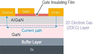
Si MOSFETs utilize a vertical structure, whereas GaN HEMTs adopt a lateral structure.
GaN is epitaxially grown on an Si substrate, after which an AlGaN (Aluminum Gallium Nitride) layer is formed.
The growth of a thin AlGaN film on GaN results in a piezoelectric effect, causing electrons to gather at the interface.
This forms a high-mobility two-dimensional electron gas (2DEG) layer that serves as a path for current to flow.

Si substrates are preferred due to their larger wafer sizes that make them easier to mass produce compared to other materials.
At the same time, the large difference in thermal expansion coefficients between GaN and Si can cause substantial stress during cooling after crystal growth, potentially leading to cracks in the substrate.
A buffer layer is provided to relieve this stress.
Switching Loss
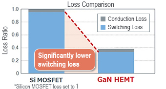
GaN HEMTs dramatically reduce switching loss compared to silicon MOSFETs.
This translates to significantly improved efficiency in power supply systems.
GaN HEMTs significantly reduce switching loss vs Si MOSFETs

Characteristics Comparison
The following table compares key characteristics of 650V-class power devices: Si SJ (Super Junction) MOSFETs, SiC MOSFETs, and GaN HEMTs.
GaN HEMTs provide superior switching characteristics in the medium voltage, medium power range.
| Si SJ MOSFET | SiC MOSFET | GaN HEMT | |
|---|---|---|---|
| Breakdown Voltage | 650V | 650V | 650V |
| Large Current Compatibility | 〇 | 〇 | △ |
| High-Speed Switching | △ | 〇 | ◎ |
| Ron・Qg*1 | 1*2 | 0.63 | 0.1 |
| Switching Speed | 1*2 | 2 | 10 |
| Qrr*3 | 0.73μC | 0.25μC | 0nC |
*1:An indicator of switching performance. The lower this value is, the better the switching performance.
*2:With silicon SJ MOSFET Ron・Qg and switching speed set as 1.
*3:GaN HEMTs utilize a structure that eliminates the parasitic PN junction between the drain and source, preventing charge accumulation during reverse conduction.


