Mask ROM <Semiconductor Device Principles>
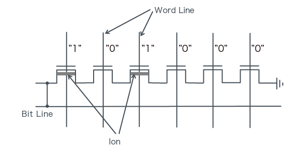
Mask ROM Memory Cell Configuration
Adopts a NAND structure for increased integration (1 transistor cell).

Data Write Method
- Information written in the wafer process
- '1' : Ions implanted in the transistor
- '0' : No ion implantation
Data Read Method
- Word line potential of the Read Cell is 0V
- Word line potential of non-Read Cell is Vcc
- Voltage is supplied to the Bit Line
- '1' is determined if current flows


