
Thin-Film Piezo MEMS Foundry
In addition to conducting R&D for many years, ROHM is focused on technological innovation using ferroelectrics. ROHM's thin-film piezo MEMS foundry utilizes in-house high reliability production equipment leveraging market-proven ferroelectric expertise along with a heterogeneous material management system that makes it possible to integrate thin-film piezoelectric MEMS and IC microfabrication technologies. At the same time, joint development allows customers to achieve next-generation solutions featuring breakthrough miniaturization with unprecedented energy savings and performance.
What is ‘piezo’? What is MEMS? -Electronic Basics
Here we explain the basics, characteristics, applications, structures, and properties of piezo and MEMS.
Development / Production Contracting
Main Technologies and Services
We provide comprehensive support from prototyping and development to mass production, including process planning for MEMS devices using silicon and SOI wafers, manufacturing high-performance piezoelectric films, and subcontracting and design support for piezoelectric MEMS devices. Feel free to contact us to discuss individual processes not listed on our website or catalogs.
Thin-Film Piezo Technologies

- ・Sol-gel PZT
- ・PZT Doping
- ・Crystallinity Control, etc.
Semiconductor Process Technologies

- ・Lithography
- ・Etching
- ・Sputtering, etc.


Mass Production and Development Line
A 6-inch MEMS line is being built at LAPIS Semiconductor’s Miyazaki Plant that integrates proprietary thin-film piezo technologies into an LSI production line.


| Location | Kiyotake-cho, Miyazaki City, Miyazaki Prefecture, Japan |
|---|---|
| Clean Room | 1,360m2 dedicated to Piezo MEMS |
| Clean Rating | Class 1-1,000 |
| Wafer Diameter | 6-Inch |
| Services Provided | Engineering samples, mass-production |
| ISO Certifications | ISO9001, ISO14001 |
| Development / Production Experience | Actuators, sensors |
| Process Technologies | PZT piezo thin film, double-sided Si processing, wafer-to-wafer bonding |
Flow from Customer Consultation to Mass Production
Our foundry with dedicated MEMS line allows us to handle everything from prototyping to mass production of customer products.

*The above flow is just an example. The actual flow will be determined after consultation in each case.
For inquiries, requests, and/or consultation, please feel free to fill out the form on the contact page.
In-House Equipment
By installing the necessary equipment and analysis tools for MEMS processes in our manufacturing line, we can propose processes for a wide range of devices and initiatives to improve quality.
| Process Category | Equipment |
|---|---|
| Deposition | |
| Sol-gel (PZT) | |
| PE-CVD (SiO2, SiN) | |
| LP-CVD (SiO2, SiN, poly-Si) | |
| Thermal Oxide Furnace | |
| Sputter (Pt, Ir, IrO2, AlCu, Ti, TiN, etc.) | |
| ALD(Atomic Layer Deposition) (Al2O3, SiO2, Ta2O5) |
|
| Water-Repellent Coating Formation | |
| Photolithography | |
| Resist Coating / Development | |
| MPA (Mirror Projection Aligner) | |
| Double-Sided Aligner, IR Stepper, i-Line Stepper | |
| Dry Etching | |
| Si Deep Etching | |
| Isolation Layer RIE Equipment | |
| PZT / Electrode ICP Etcher | |
| Wet Etching | |
| SiO2 Etching | |
| Au Etching | |
| Si Anisotropic Etching | |
| Wafer Bonding | |
| Resin Bonding | |
| Anodic Bonding |
| Process Category | Equipment |
|---|---|
| Tape Lamination | |
| Automated Wafer Tape Bonding Machine (UV Tape, Thermal Release Sheet, Polyimide, etc.) |
|
| Stripping and Cleaning | |
| Asher | |
| Organic / Polymer Stripper | |
| Acid Cleaning, Scrubber | |
| Dividing, etc. | |
| Dicing, Two-Fluid Cleaning | |
| Circle-Cut Dicer | |
| Measurement | |
| Analysis / Measurement SEM, Ion Milling | |
| Optical Measurement Equipment | |
| Front / Back Misalignment Measurement Equipment | |
| Visible Light / IR / Laser Microscopes | |
| X-Ray Diffractometer | |
| Laser Displacement Measuring Device | |
| X-Ray Fluorescence (XRF) Analyzer | |
| Needle / Optical Interference Type Step Gauges | |
| Ellipsometer | |
| Automated Visual Inspection Equipment (Compatible with Front/Back Through-Wafers) | |
| Electrical Characteristics Evaluation Devices (i.e. Probes, Testers) |

Process Capabilities
Feel free to contact us to discuss individual processes not listed on our website or catalogs.
| Process | Process Specifications | Value | Comments |
|---|---|---|---|
| Photolithography | Minimum Line Width (with Stepper) Minimum Line Width (with Aligner) |
1μm 3μm |
|
| Si Deep Etching | Taper Angle Etching Rate In-Plane Uniformity Dimensional Accuracy |
90+/−1˚ ≤5% +/−0.1μm (Both are pattern-dependent) |
Through-Substrate Processing Possible Processing on Both Sides (Front / Back) Enabled (Notch-free) Optional Taper Control |
| TMAH Etching | Depth | ≤In-plane 5% | Through-Substrate Processing Possible Processing on Both Sides (Front / Back) Enabled |
| PZT Deposition | Film Thickness Accuracy | In Wafer: +/−1.0% Between Wafers/Lots: +/−2.5% |
Doping Ex. (Nb, La) |
| PZT Etching | Processing Line Width Accuracy Etching Rate In-Plane Uniformity |
+/−1μm ≤5% (PZT thickness −3μm, tapered shape available) |
Pt stop enabled |
| Sputtering | Thickness Uniformity | ≤In-plane 4% | Pt, Ir, IrO2, AlCu, Ti, TiN, etc. |
| CVD | Thickness Uniformity | ≤In-plane 4% | SiO2, SiN |
| ALD | Thickness Uniformity | ≤In-plane 5% | Al2O3, Ta2O5, SiO2 |
| Resin Bonding | Alignment Accuracy Resin Thickness |
+/−5μm 1 to 3μm |
Epoxy, BCB |
| Anodic Bonding | Internal Seal Pressure | >0.01Pa | Si / Glass |
- PZT Film Performance
[PZT Stack Cross-Section] - Wafer-Level Bonding
[Wafer Bonding Cross-Section] - Si Deep Etching
[400μm Si Penetration] - ALD Protective Film Formation
[Silicon Shaped Cross-Section]
Examples of Prototypes / Mass Production Results
Leveraging experience in mass-producing inkjet heads along with expertise in MEMS technology allows us to collaboratively develop and evaluate prototype actuator devices requiring low power consumption and high displacement in a compact size.


Process Technology Examples
PZT Film Performance

[PZT Stack Cross-Section]
In 1998 ROHM was the first in the world to successfully mass produce ferroelectric memory.
We also possess many years of experience and expertise in the use of thin-film on silicon wafers.
The result is a sol-gel PZT film (deposited using in-house equipment) that achieves industry-leading piezoelectric performance and reliability.
| Parameter | Value | Conditions |
|---|---|---|
| Piezoelectric Constant e31, f (−C/m2) | 19 | 10V/μm |
| Inverse Piezoelectric Constant d31 (−pm/V) | 260 | 10V/μm |
| Isolation Voltage (V/μm) | >75 | Room temperature (Restricted due to evaluation power supply) |
| Isolation Life (years) | >10 | 20V/μm, 105˚C, (Estimation via acceleration testing) |
| Repeat Life (times) | >1x10¹⁰ | 10V/um, displacement reduced 10% (Unipolar pulse) |
| Leakage Current Density (A/cm2) | <1x10⁻⁷ | 20V/μm |
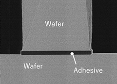
Wafer-Level Bonding Technology

[Wafer Bonding Cross-Section]

[Wafer Bonding Cross-Section / Step Region]
Multiple silicon wafer bonding technologies allow us to perform wafer-level bonding even for devices with complex structures.
*We can propose adhesive application and bonding processes.

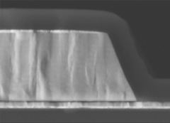
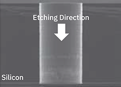
Si Deep Etching

[400μm Si Penetration]

[Silicon Wafer Processing]
We utilize multiple Si deep etching equipment from different companies (including some developed in-house) to propose the optimal Si etching process (shape, tolerance, foreign particle level, cost) for each product.

Thin Wafer Handling Technologies

[Thin Silicon Wafer]
We developed in-house wafer transport equipment that enables processing and wafer bonding using thin silicon wafers.


[TAIKO Ground Wafer]

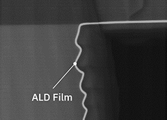
ALD Protective Film Formation

[Silicon Shaped Cross-Section]
ALD* can form a uniform protective film even on devices with complex uneven shapes.
*ALD:Atomic Layer Deposition
Protective Film: Protects devices from external factors (i.e. ink, abrasion caused by contact, static electricity).
Click here for a detailed explanation of ALD -Electronic Basics
Simulation Analysis of Piezoelectric Devices

[Silicon Cantilever Cross-Section]
We can perform finite element simulations of piezoelectric devices to propose optimal structures and processes.
