What is a Load Switch?
A load switch is an electronic component that has no moving parts, which works somewhat like a relay. Generally, two MOSFET transistors act like a switching element, one of them being an N-channel device, and the other a P-channel device.
Below we will cover when that switching element is either ON or OFF, and what that entails.
Inrush Current When the Load Switch is ON
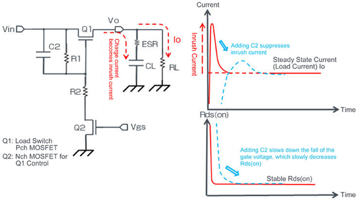
When the load switch (Q1 in the diagram below) is turned ON, a large current much greater than the steady-state current will temporarily flow. If the charge on the capacitor is close to zero then a large inrush current occurs, voltage is supplied to the output Vo, resulting in an instantaneous and large charge in current flow. This excessive current is often referred to as inrush current.
The peak of the inrush current is largely determined by the input voltage Vi, Rds(on) of the Q1 MOSFET, and the ESR of the load capacitance CL on the load side, and increases along with the input voltage Vi. Excessively large inrush current can cause system failures or malfunctions. Exceeding the maximum rated current can also result in destruction.
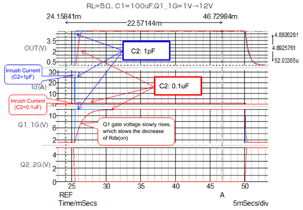
However, by adding a C2 capacitor in parallel with the R1 resistor connected between the Gate and Base of the Q1 MOSFET it is possible to slow the decrease of the Gate voltage, which will gradually reduce Rds(on) and suppress the inrush current.
Load Switch Equivalent Circuit Diagram

Inrush Current Countermeasure (When the Nch MOSFET Load Switch is Turned ON)
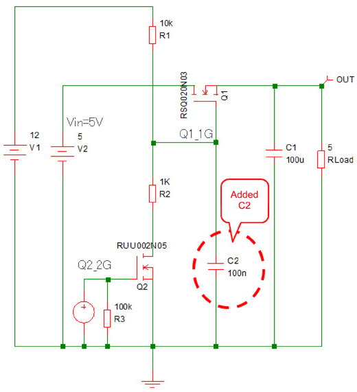
Nch MOSFET Load Switch: RSQ020N03
Vin=5V, Io=1A, Q1_1G=1V?12V
- The load switch Q1 is ON when Q2 is OFF (the Q1 Gate voltage will be greater than Vo (Q1 Vgs))
- The load switch Q1 is OFF when Q2 is ON
- As a countermeasure, C2 has been added to minimize inrush current when Q1 is turned ON
Nch MOSFET Load Switch Equivalent Circuit Diagram


Reverse Current When the Load Switch is Turned OFF
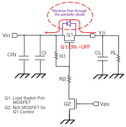
Even when the load switch Q1 is switched from ON to OFF, voltage at the output Vo pin will remain for a certain period of time based on the load capacitance CL at the output side.
If the voltage at Vi is lower than Vo, reverse current may flow from the Vo output to the Vin input through the parasitic diode formed between the Q1 MOSFET Drain and Source. Make sure that the rated current of the Q1 MOSFET is never exceeded under any circumstances. In addition, consider the rise timing, taking into account the load conditions, when determining the capacitance value of the input bypass capacitor CIN.
Load Switch Equivalent Circuit Diagram


