memory_what2
Types of Memory
<Semiconductor Device Principles>
Numerous types of memory exist for Semiconductor memory Device. Basic types of memory sich as 'DRAM', 'SRAM', 'Mask ROM', 'EEPROM' and 'Flash Memory' are explained below.
DRAM
Memory Cell Structure
Consists of 1 Transistor and 1 Capacitor.
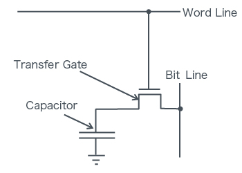
Data Write Method
In the Case of '1':
- Word Line potential is High
- Bit Line potential is High
- Word Line potential is Low
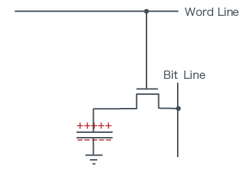
The state of '1'
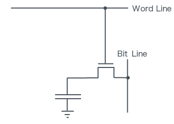
The state of '0'
SRAM
Memory Cell Structure
- 6-Transistor Cell Configuration
- 4-Transistor Cell Configuration (High Resistive Load Cell Type)

Low Power Type to the left, High Density Type to the right.
Data Write Method (see diagram below)
In the Case of '1':
- Word Line potential is High
- Assign a potential to the Bit Line (D=Low, D=High)
- The state of the flip-flop
- Word Line potential is Low
Data Read Method
In the Case of '1':
- Word Line potential OFF
- Bit Line precharge (same potential as D, D)
- Word Line potential is High
- If the Bit Line is Low the conditions will be High
- Amplified by the sense amp

The state of '1' to the left, The state of '0' to the right. '0', '1' stored by the flip flop circuit
Mask ROM
Mask ROM Memory Cell Configuration
Adopts a NAND structure for increased integration (1 transistor cell).

Data Write Method
- Information written in the wafer process
- '1' : Ions implanted in the transistor
- '0' : No ion implantation
Data Read Method
- Word line potential of the Read Cell is 0V
- Word line potential of non-Read Cell is Vcc
- Voltage is supplied to the Bit Line
- '1' is determined if current flows
EEPROM
EEPROM Memory Cell Configuration
Consists of 2 transistor cells.

Data Write Method

Data Erase Method

Flash Memory
Flash Memory Cell Configuration
- NAND Type

4F2 area per bit when the minimum rule is F
- NOR Type

10F2 area per bit when the minimum rule is F
Data Write Method

Data Erase Method