Stories of Manufacturing#04
Transforming
ROHM’s unique
‘strengths’ into ‘trust’Wafer Production Process
Core Plant for Analog ICs
Blessed with a mild climate and abundant water resources, Hamamatsu is a land known for nurturing world-class companies that manufacture products such as musical instruments and motorcycles, along with a textile industry that has continued uninterrupted since the Edo period.
ROHM Hamamatsu Co., Ltd. began operations in 1999 as a core plant responsible for the front-end processing of ROHM ICs and LEDs. Over the years, we have launched products tailored to the needs of each era, quickly responding to the emergence of the digital market, market globalization, and shifting trends toward a decarbonized, recycling-oriented society.
Equipped with advanced device and process technologies and production facilities specializing in ROHM’s strength in analog ICs, more than 70% of ROHM’s ICs are produced here. The plant, which utilizes two production lines for 8- and 12-inch wafers, ships more than 50,000 wafers a month. (*8-inch conversion)
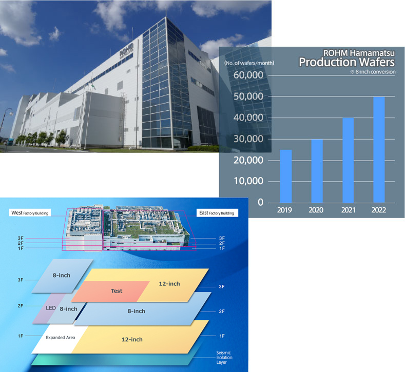
ROHM Hamamatsu Co., Ltd.( Hamamatsu City, Shizuoka Prefecture)
Consists of two factory buildings on a site of approximately 62,000m2.
The world’s first semiconductor factory to adopt a seismic isolation structure.
The total floor area is approximately 30,000m2, and the combined length of the corridor running through the center of the clean rooms of the factory and west factory buildings is approximately 160m, where more than 1,000 types of ICs are produced.
In addition to mass production lines, we have achieved high mix high volume production using a complex manufacturing system that combines multiple production lines to meet various customer needs.
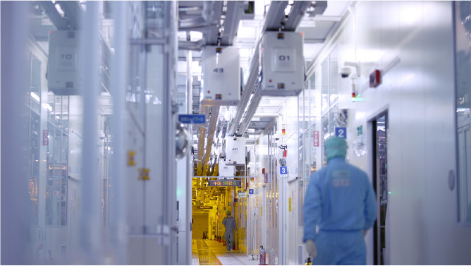
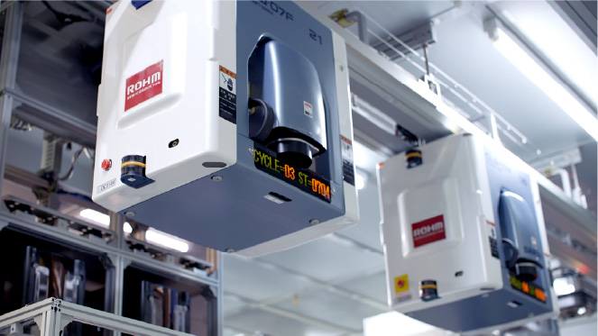
Pods holding 24 12-inch wafers traverse the clean room overhead.
The distance traveled on average is 25km from entry to shipment.
Together with Evolution of a Mobile Society
Currently, among ROHM Hamamatsu’s production lineup, automotive products stand out in terms of production volume. Involved in this field since it was established in 1999, ROHM Hamamatsu has gradually gained the trust of customers, with automotive products now accounting for 60% of total production.
Following the dramatic increase in the number of electronic components caused by the shift to EVs and HEVs - which is considered to be a once-in-a century revolution - together with the widespread adoption of ASVs (Advanced Safety Vehicles) and evolution of autonomous driving, the demand for automotive products is expected to continue to rise sharply.
At the same time, however, as automotive products are directly related to the safety of the end user, product safety and reliability standards are understandably very strict. (Ex: AEC-Q100, IATF 16949, ISO 26262)
ROHM Hamamatsu has supplied more than 3 billion ICs to customers around the world. This figure, accumulated over many years, is a testament to our thorough quality control and ability to meet the most stringent standards.
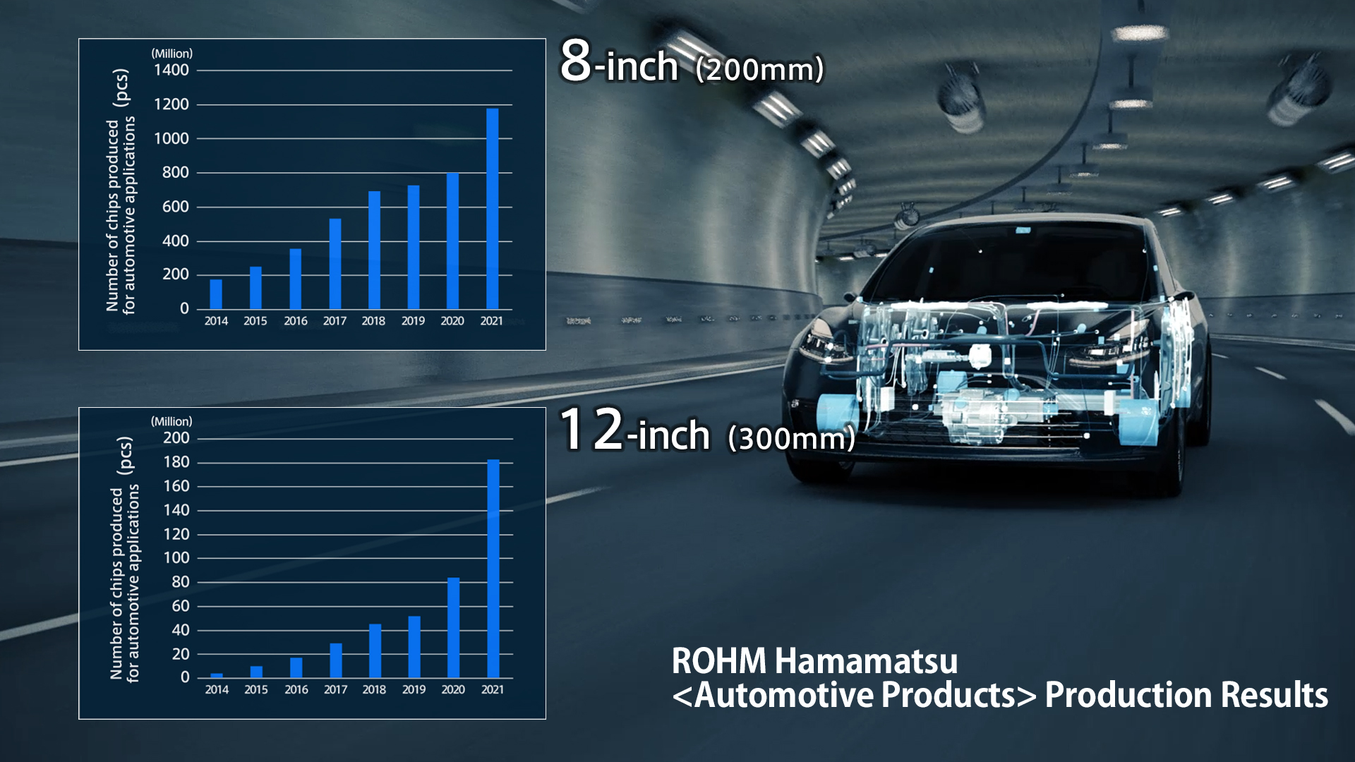
ROHM Hamamatsu’s Automotive Production Results
The number of chips produced in 2021 reached to approx. 1.4 billion
It has grown sevenfold from 2014 to 2021.
Needless to say, this is not a market where simply meeting the required specifications is enough to guarantee adoption.
We asked Mr. Yamashita of the Manufacturing Div.1, LSI Manufacturing Headquarters how the company was able to win customer trust and grow into a field that can be called the mainstay of today's production.
Challenges towards 12-inch (300mm) BiCDMOS
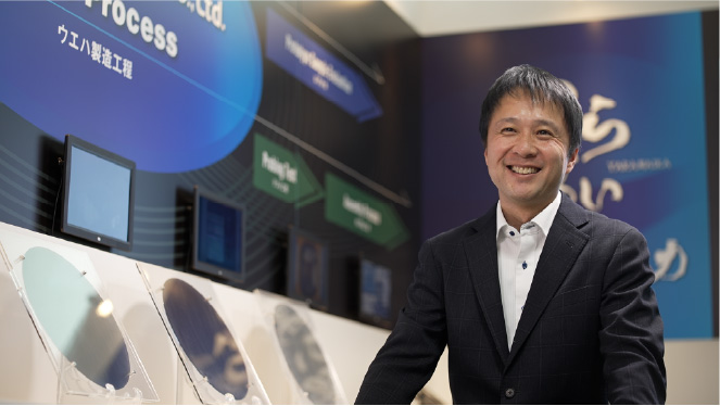
ROHM Hamamatsu Co., Ltd.
Manufacturing Div.1, LSI Manufacturing Headquarters
He began his days at ROHM Hamamatsu at the ‘beginner’ level of ‘What is a semiconductor?’
And is grateful for an environment that encouraged self-growth.
With a wry smile, Mr. Yamashita mentioned that this would never be possible under today’s current working system.
‘If I were asked to do it again, it might be tough to be honest,’ he prefaced, but he was convinced that taking on this challenge formed the foundation for the entire ROHM Hamamatsu BiCDMOS process.
On-site capabilities that support innovation
ROHM’s unique ‘strength’ was behind the decision to take on challenge of the ‘12-inch BiCDMOS process’, which has yet to be achieved by any major global company.
This in-house development technology for manufacturing equipment has been continuously nurtured since the company was founded. ROHM Hamamatsu has created a unique production line that balances in-house production equipment optimized for processes with purchased equipment optimized in collaboration with engineers from the equipment manufacturers.
When the 12-inch production line was first launched, most of the equipment was developed in-house, making it possible for us to come up with the starting point for the challenge on our own.
We asked Mr. Taniguchi of the Equipment Engineering Dept.1, Manufacturing Div.1, LSI Manufacturing Headquarters, to look back on those days.
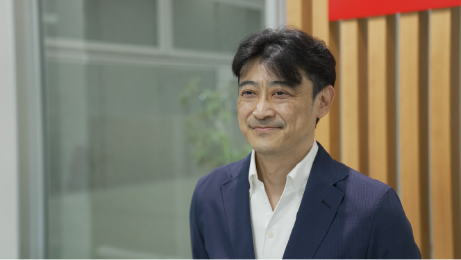
ROHM Hamamatsu Co., Ltd.
Equipment Engineering Dept.1, Manufacturing Div.1,
LSI Manufacturing Headquarters
He does almost all of the maintenance on his favorite bike himself.
And cherishes the feeling that taking care of things using tools for that purpose is protecting him.
Taniguchi:
‘High temperature processing is a crucial step in the BiCDMOS wafer process, but there was the problem of silicon distortion invariably occurring with 12-inch wafers.
Therefore, by reviewing the component design of the heat treatment furnace, we were able to perform treatment at an ultra-high temperature of 1200°C, which exceeds the general high temperature limit.
We were able to break through this barrier using the knowledge of our engineers, who possess a deep understanding not only of the equipment, but also the wafer process itself, passed down from generation to generation. The ‘intuition’ to immediately identify the location and cause of defects is something that cannot be acquired overnight.’
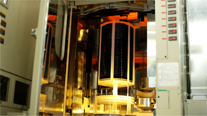
Deposition process of ion implanted wafers in an ultra-high temperature heat treatment furnace.
Improving and maintaining the manufacturing equipment can significantly affect the quality of wafers.
What’s more, it is said that one of the major factors is that the device, process, and equipment sections were able to work together on this development project within a vertically integrated production system, which is one of ROHM’s strengths.
‘On-site’ capabilities that can overcome various technical challenges...
This is perhaps ROHM Hamamatsu’s greatest ‘strength.’
The following is a development episode that confirms this.
Front loading and quality assurance
Isolated gate driver ICs that control power devices responsible for driving the main motor in EVs/HEVs. The first in the world to mass produces these products in 2016, which are considered essential for next-generation mobility, ROHM has since gained the top market share.
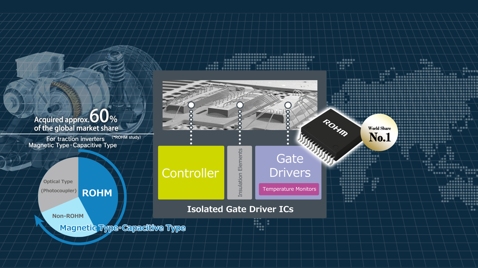
Utilizing a magnetic method for isolation instead of optical (photocoupler) achieves breakthrough
miniaturization with a single-package design.
However, it took more than a year of hard work to gain the trust of customers in adopting this completely new product. Mr. Wada, in charge of the Technology Development Segment, LSI Business Unit. who was involved in the project, shared his thoughts.
Wada:
‘We had to assume a high level of risk as it is an automotive component involved in the core of the main motor drive. In the event of malfunction, the safety of the end user is at stake, so it was necessary to ensure ‘quality after considering all risks.’’
One example is the risk of particles during production.
At ROHM Hamamatsu, manufacturing is based on the premise of ‘no foreign matter’ in all phases, beginning with plant design, equipment management that includes preventive maintenance, and process conditions. Measures are also taken to detect product failures by sorting using defect inspection machines and conducting screening tests before shipment, but there have been cases where questions were asked,such as ‘What would happen if particles were mixed in?’ and ‘Does the screening process really work as designed?’
The process of trial and error can be seen in the video at the beginning of this slide, so he was asked again about his thoughts on ‘quality’ obtained here.

Process Development Dept., LSI Device Development Div.,
Technology Development Segment, LSI Business Unit
Having worked in the manufacturing department for a short period of time after first joining the company, he remarked, ‘I think I understand some of the difficulties involved.’.
On his days off, with a spirit of craftsmanship he challenges himself by making elaborate dishes such as making buckwheat noodles from the buckwheat flour.
Wada:
‘For one thing, it was a valuable experience in terms of how to ensure quality and gain the trust of customers. In addition to quality assurance, which we have built up through front loading, we must also manage risk with the future in mind.
The other is the technology and system to resolve any question or concern the customer may have. I can proudly say that all of these together comprises ‘our quality.''
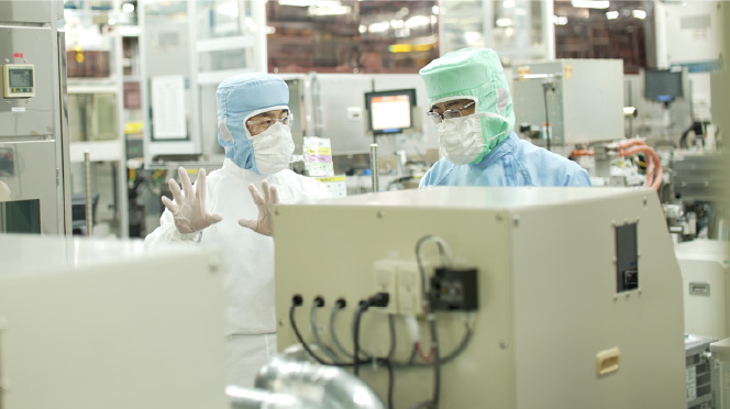
To demonstrate the effectiveness of the screening test, wafers ‘intentionally’ created with particles were manufactured over a period of several months.
Through this project, all members were able to once again share the weight of social responsibility in semiconductor manufacturing.
Mr. Wada is stationed at ROHM Hamamatsu as part of the development section, leading a team that includes engineers specializing in process design, simulation, mask design, and measurement/analysis. In addition to improving the technical capabilities of his own team, he is also focused on ‘building close relationships’ with the manufacturing section responsible for production and equipment.
Wada:
‘One of our advantages is that our departments are located in ROHM Hamamatsu in close proximity to one other. What’s more, even now, if there are issues with a product that is being mass produced, the manufacturing department consults with us and we work together to find solutions.
I feel that being physically close is actually very important in terms of improving quality.’
Development and manufacturing work together to resolve questions and concerns from customers This kind of system is undoubtedly a unique advantage of ROHM’s vertically integrated structure. But more than that, it seems that the ‘passion’ that arises when the company moves in one direction can lead to customer ‘trust.’
Beyond ‘Quality First’...
Yamashita:
‘The other day, a customer came to us for a new part adoption audit, and mentioned that being honest and responsive were the reasons ROHM was selected.
He said that our strength lies not in the fact that we ‘provide the specifications our customers want’, but that we work together with our customers to diligently respond to various issues that arise at their sites.
At that time, what came to Mr. Yamashita’s mind was ROHM’s corporate objective of ‘Quality First.’ He says that he realized once again that ‘quality first’ doesn’t simply mean supplying products with good characteristics or making large quantities of good products, but rather satisfying our customers and the end users beyond those customers.
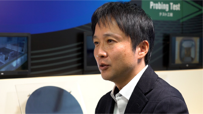
‘When I heard the customer say ‘honesty is ROHM’s strength’, I almost felt overwhelmed.
I immediately went to tell all of the members at the factory.’
Yamashita:
‘We have been operating a wafer factory for over 20 years, but the employees at the factory inevitably feel distant from the customers. What’s the purpose of what we’re making? We provide an opportunity for all employees to think about this question together.’
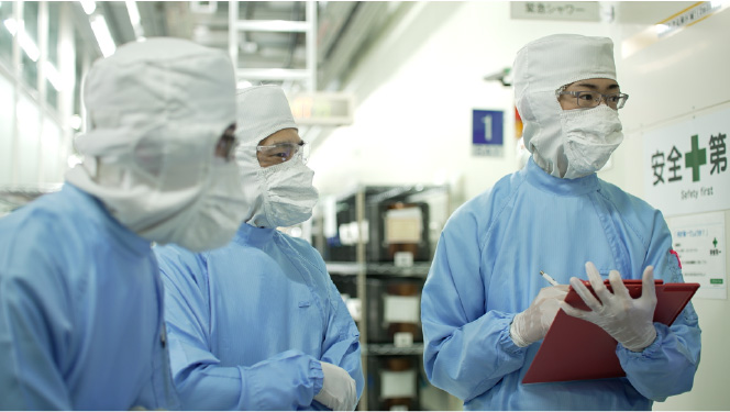
About 800 employees work at ROHM Hamamatsu. (*As of May 2023)
The spirit of challenge that embodies the local Enshu dialect, ‘Yaramaika! (Let’s try it!)’ is a source of our on-site capabilities.
It is not easy to reconsider the fundamental meaning of manufacturing at a production plant, where the daily routine tends to fall into the trap of prioritizing efficiency and compliance with rules and regulations.
To becoming a group that creates ‘satisfaction for those down the line’ from each product...
This determination starts with listening to someone else’s voice like today, leading us into the future.
Toward a world created by next-generation semiconductors
ROHM Hamamatsu is currently in the process of expanding the 12-inch line, which is slated to begin operation in July 2023 to further increase production volume.
And as a new technology, we are gradually developing a ‘thick-film Cu rewiring process’ for our 12-inch line to meet market needs for even higher current, with plans to release 0.13μm BiCDMOS equipped with DTI (Deep Trench Isolation).
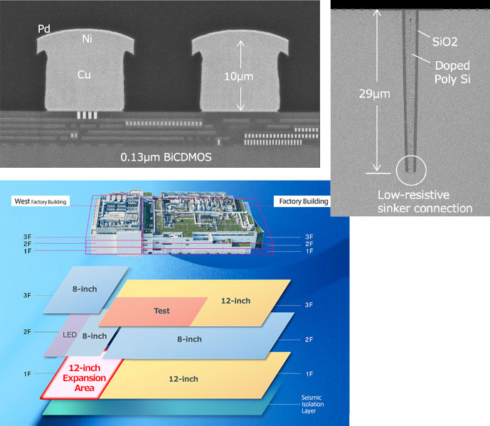
Thick-Film Cu RDL (Redistribution layer) Process
DTI (Deep Trench Isolation)
Yamashita:
‘The automotive field is in the midst of a technological revolution. We believe that our mission is to always provide the reliability and quality our customers demand at any given time...or even exceed their demand.
We hope to contribute to a new world created with next-generation semiconductors by firmly linking our ’strengths‘ to the voices of our customers!’
Related Link(s)
ROHM Hamamatsu Co., Ltd. https://micro.rohm.com/en/hamamatsu/


Yamashita:
'Not limited to just automotive products, but for over 20 years we have always taken on the challenge of manufacturing with a focus on quality. A major driving force was the world’s first mass production using a 12-inch BiCDMOS process in 2009.