

Stories of Manufacturing#05
Endless struggle
against invisible noiseEMC Countermeasure Design
ROHM’s EMC Measurement Site
ROHM’s Yokohama Technology Center as seen from the Shinkansen at the Shin-Yokohama Station. The door at the end of the first floor of the open-plan building filled with glass surfaces opens up to an entrance to what seems to be an independent facility, with several rooms located at the end of the corridor.
This facility, which is visited daily by many engineers, including in-house device designers and customers, is an EMC measurement site that supports ROHM’s analog IC development.

▲Yokohama Technology Center (Yokohama City, Kanagawa Prefecture)
▲EMC Measurement Site Plan Layout ▶
EMC measurement sites, which include facilities accredited and operated by the Japan Quality Assurance Organization (JQA) as well as laboratories owned by major electrical manufacturers and specialized companies located throughout Japan, were established for the purpose of measuring and testing the effects of electromagnetic noise emitted from a wide variety of electrical and electronic equipment, wireless devices, and information communication systems. However, it is rare in Japan for a semiconductor manufacturer to establish and continue to operate its own testing facility.

Triangular radio wave absorbers are attached to the walls of the 3m radio wave anechoic chamber to prevent the reflection of radio waves in the room
Increased noise sources/Associated development person-hour
In 2009 ROHM created a unique facility with two anechoic chambers designed and constructed to be unaffected by external electromagnetic waves while also preventing electromagnetic waves from leaking to the outside.
We asked Mr. Ogawa, who has been involved at the site from that time, about how it all began.

Circuit Technology Development Division.
LSI Business Unit Group Leader Osamu Ogawa Osamu
Ogawa
Mr. Ogawa was originally an LSI design engineer before assuming his current position.
He mentions that his past knowledge has been very useful in suggesting measurement methods and providing advice on circuit design.
Noise problems are beginning to cast a shadow as a major destabilizing factor for the development departments of various electrical and electronics manufacturers.
The background to this coincided with discovery of the noise issue.
Ogawa:
‘In most cases, problems caused by noise are found when sample products are evaluated in the customer's set after operation verification of the IC itself has been completed.
But it is sometimes difficult to determine the cause of the problem, since frankly we have no idea what other components are used or what position they’re in.
In any case, there's almost nothing that can be done to the IC at that point. So we end up having to go back and redesign with countermeasures.’
To avoid an increase in person-hour and scheduling conflicts this entails, there is a growing need for high accuracy EMC measurements at an early stage during development.
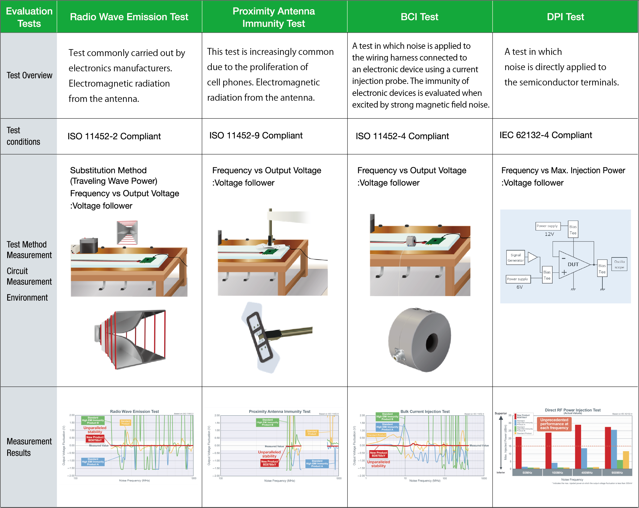
2 EMC Measures and Measurement Support
Ogawa:
‘EMC design can be broadly classified into two categories: the first is that ICs must not malfunction due to noise from other sources (immunity=EMS), and the second is that IC circuits must not become a source of noise (emissions=EMI). At our EMC site we offer a wide range of testing services for both of these types, depending on the request.’

Immunity=EMS
Emission=EMI
EMC needs to account for both of these factors
Noise measurements are also performed in the automotive anechoic chamber by reproducing both the placement and mounting distance in the vehicle, including the wiring harnesses. Using multifaceted methods allow us to achieve high accuracy measurement results that take into account the mounting environment.

Automotive Anechoic Chamber
Various vehicle standard tests are conducted by placing wiring harnesses on a desk that simulates the body of a car.
Ogawa:
‘We propose what measurements should be taken first while sharing the current issues with the designer. Based on the measurement results, the core of our job is to talk with designers in a consulting capacity and ask questions like ‘Why is there so much noise?’ and ‘Which direction should we take to improve?’
By having IC designers and engineers at our in-house EMC measurement site work together on a single issue, a unique virtuous cycle is created that allows us to reach the desired results in the shortest possible time.
Now, let’s talk specifically about the process from the perspective of a design and development engineer that led to the commercialization of an ‘ultra-high EMI tolerance op amp’ born through close collaboration.
Automotive Op Amps that Pursue a Completely Noiseless Design
Makimoto:
‘The part I am working on is called an op amp that amplifies weak signals from sensors, and is susceptible to noise that if picked up can induce malfunctions and misjudgments which can lead to serious accidents.
This is why in recent years the industry as a whole has seen an increasing demand for op amps featuring high noise immunity.’

Circuit Technology Development Division.
LSI Business Unit Engineer Hiroyuki Makimoto Hiroyuki
Makimoto
Mr. Makimoto majored in electrical engineering and conducted research on IC failure diagnosis. After joining the company, he was part of the NFC (Near Field Communication)project involved in the establishment of wireless power supply standards.
The latest cars are being controlled by several ECUs that use sensors to detect environmental changes such as temperature, pressure, and brightness. With the addition of automated driving and mobile communications, all types of electronic components are being miniaturized and densely packed, making the radio wave and noise environments inside the car quite severe.
Under these conditions, Mr. Makimoto’s challenge to develop an op amp that doesn’t malfunction even when subjected to noise was quite bold.
Makimoto:
‘Certainly, it has been difficult to improve noise immunity...an area that even our competitors have not been able to tackle. To be honest, I thought it would be impossible at first, but thanks to the active cooperation of members at the EMC measurement site, we were able to create a mindset of ‘Let’s take on the challenge anyway’.

Tests conducted during the development of ultra-high EMI immunity op amps.
This has become a powerful backbone for products that can handle all types of noise.
▶Click to magnify
Mr. Kurokawa, the engineer who actually conducted this series of tests, recalls his conversation with IC designer Mr. Makimoto as follows.
Kurokawa:
‘We brought various circuit proposals to the anechoic chamber as prototypes, where we conducted repeated measurements and verification.
These efforts continued for some time, and one day when there was an opening in the schedule of the anechoic chamber we tried one of the rejected prototypes ‘by accident’, which turned out to have outstanding noise immunity.’

Development Division V&V Engineering Dept.
EMC Grp. Engineer Yoichi Kurokawa Yoichi
Kurokawa
Acquired iNARTE EMC Certification by the International Association for Radio, Telecommunications, and Electromagnetics, a non-profit membership/certification organization.
Enomoto:
‘I can’t believe it happened this way! It was a circuit proposal that made everyone around me shake their head in disbelief, and if it had been a normal schedule, we wouldn’t have even tried it as it was a rejected idea (laughs).’
Of course, this was only possible due to a thorough review of the circuitry, layout, element, size, and other factors, but it was also surprising how it seemed to be guided by the ‘good luck’ of Mr. Makimoto and members of the EMC measurement site.
This circuit proposal resulted in the EMARMOUR™ series of op amps featuring the industry’s highest class noise immunity, which are still active in market, where they have been adopted by numerous manufacturers.

Contributes to reducing the number of peripheral components and person-hour required for noise countermeasures, lowering costs while shortening delivery times for set design
Related Link(s)
EMARMOUR™
: https://www.rohm.com/emarmour
Combatting switching noise
At the same time, many engineers are making steady efforts on a daily basis to prevent EMI=self-generated noise.
Here, we will focus on DC-DC converter ICs for use as automotive components.
The continuing proliferation of EVs/HEVs and integration of peripheral equipment that includes communication devices and sensors have led to an increasingly diverse range of voltage conversion in vehicles. What’s more, higher performance resulting from improved conversion efficiency and high-speed response is required, while reducing both the size and weight of components themselves have become a significant challenge.
In addition to product development under such harsh conditions, a major safety concern for design engineers is high frequency noise generated during switching.
The higher the switching frequency, the easier it is to achieve faster response and smaller element size, but how can we overcome the trade-off where more noise is generated as switching speed increases? This has become a major mission for design engineers.
Oshita:
‘For automotive components in particular, ICs are valued for their small size. As today's vehicles are equipped with a veritable mountain of such ultra-compact ICs, the risk of malfunction due to the noise they generate increases year by year.’

Power Management LSI Division.
LSI Business Unit Engineer
Hiroto Oshita Hiroto
Oshita
Mr. Oshita stands out by wearing a necktie where business casual is the norm. This cool demeanor is reflected in the circuits he designs.
Mr. Oshita, a design engineer whose main focus is power supply ICs, speaks in a calm tone.
The effects of noise in vehicles can range from interference and desensitization of communication equipment such as radios and GPS to impacting speakers when issuing danger alerts and even motor malfunctions.
In the latter half of the 2010s, we reflected on our predicament as we faced the demand from customers wanting to drive ICs at a high frequency of 2MHz and the introduction of the new automotive standard CISPR25.
Oshita:
‘The noise performance we had achieved in the circuit design and simulation on the PC didn’t work when we implemented it in the car, so we had to carry out a number of redesigns. After all, a lot still depends on the surrounding conditions, such as the board and placement of components.
In the end, we created about 20 types of PCBs, brought them to the anechoic chamber, measured them, received feedback from EMC measurement site members, then made the necessary modifications. This cycle was repeated many times.

DC/DC Converter EMI Measurement
▶Radiated emissions ▶Conducted emission voltage/current method
Verification from various angles is required to determine that there is no interference by noise to other vehicle systems.
Members of the EMC measurement site don’t just stop with measurement and analysis in the anechoic chamber, but also play the role of a designer by engaging in the frequent exchange of opinions with design engineers from the stage of creating boards to be tested.
As a specialist who is required to have not only expertise about noise but also an in-depth knowledge of IC characteristics and industry trends, he is considered to be indispensable in the development of semiconductor devices today.

Development Division V&V Engineering Dept.
EMC Grp. Senior Engineer Katsunori Kido Katsunori
Kido
Acquired iNARTE-EMC/EMC Design Engineer Certification by the International Association for Radio, Telecommunications, and Electromagnetics, a non-profit membership/certification organization.
Simulation development supported by extensive expertise
In recent years, expectations for simulation of noise countermeasure designs have been increasing.
The prevailing trend in the manufacturing industry is undoubtedly one that promotes speedy product development and cost reduction by solving various issues early in the development process.
In addition, as many semiconductor manufacturers are seeking a future where noise suppression is completed through simulation, ROHM envisions a transitional approach involving partial and incremental steps.

LSI EMC Design (by Ryosuke Inagaki, ROHM Co., Ltd.)
Written by Mr. Inagaki, Chief Engineer, Circuit Technology Development Dept., LSI Business Div., who has been a leader in noise countermeasures at ROHM.
Although published in 2018, many designers regard it as a bible as it is chock-full of simulation-based knowledge.
Ogawa:
‘I believe that simulation technology will be increasingly adopted in step with the evolution of AI and the application of analysis technology, but even in the process up to that point, I think the responsibility imposed on radio and noise experts like us is by no means small.’
The expectations for EMC countermeasure design, one of the key technologies driving the next generation of manufacturing, will continue to rise in the future.
Where do we at ROHM stand in the context of this, and what kind of world are we hoping to see?
The answer lies in the ongoing daily struggle against invisible noise, where the quiet determination of EMC design engineers and electronic device designers brightly illuminates the path to the future.
Ogawa:
‘Since the beginning of the 2000s, as the performance of ICs continue to improve and operate at higher speeds and frequencies, the amount of noise generated in all types of devices has been steadily increasing. The entire industry, from consumer electronics to vehicle manufacturers, has naturally become sensitive to this issue, and at the same time, international standards regulating electromagnetic radiation have become increasingly stringent and fragmented.
I think the biggest reason for launching ROHM’s own measurement site was, above all, the speed of product development. Having an environment that allows us to evaluate and assess the noise of developed products from the development stage directly relates to the peace of mind and level of trust of our customers.’