Not Recommended for New Designs
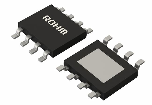
BD9G500EFJ-LA
7V to 76V Input, 5A Integrated High-Side MOSFET, Single Buck DC/DC Converter
BD9G500EFJ-LA
Not Recommended for New Designs
BD9G500EFJ-LA
7V to 76V Input, 5A Integrated High-Side MOSFET, Single Buck DC/DC Converter
This product cannot be used for new designs (Not recommended for design diversion).
Product Detail
Replacement Product For BD9G500EFJ-LA
| Part Number |
|
|
|---|---|---|
| Ordering Part Number | BD9G500EFJ-LAE2 | BD9G500UEFJ-LAE2 |
| Similar Level | - | Same Pinout, Package |
| Data Sheet | ||
| Supply Status | Not Recommended for New Designs | Recommended |
| Package | HTSOP-J8 | HTSOP-J8 |
| Unit Quantity | 2500 | 2500 |
| Minimum Packing Quantity | 2500 | 2500 |
| Packing Type | Taping | Taping |
| RoHS | Yes | Yes |
| ch | 1 | 1 |
| Integrated FET / Controller | Integrated FET | Integrated FET |
| Topology | Buck | Buck |
| Vin1 (Min.)[V] | 7.0 | 7.0 |
| Vin1 (Max.)[V] | 76.0 | 76.0 |
| Vout1 (Min.)[V] | 1.0 | 1.0 |
| Vout1 (Max.)[V] | 68.4 | 68.4 |
| Iout1 (Max.)[A] | 5.0 | 5.0 |
| SW frequency setting (Max.)[MHz] | 0.65 | 0.65 |
| Synchronous / Nonsynchronous | Non-synchronous | Non-synchronous |
| Light Load mode | No | No |
| EN | Yes | Yes |
| PGOOD | No | No |
| Operating Temperature (Min.)[°C] | -40 | -40 |
| Operating Temperature (Max.)[°C] | 125 | 125 |
| Thermal Model | /en/products/databook/applinote/ic/power/switching_regulator/bd9g500efj-la_2resistor_thermalmodel_an-e.pdf | /en/products/databook/applinote/ic/power/switching_regulator/bd9g500efj-la_2resistor_thermalmodel_an-e.pdf |
| Package Size [mm] | 4.9x6.0 (t=1.0) | 4.9x6.0 (t=1.0) |
Reference Design / Application Evaluation Kit
-
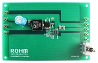
- Evaluation Board - BD9G500EFJ-EVK-001
This EVK is using not BD9G500UEFJ-LA, but BD9G500EFJ-LA. BD9G500EFJ-EVK-001 uses BD9G500EFJ-LA to output 5V from a 48V input voltage. The input voltage of the BD9G500EFJ-LA is from 7V to 76V and the output voltage is configurable from 1V to 0.97 x VIN V with external resistors. The operating frequency is configurable between 100 kHz and 650 kHz with an external resistor connected to RT pin. This is a current mode control DC/DC converter that provides fast transient response performance and simple phase compensation setup.

Videos & Catalogs

Videos
Digital Datasheet | BD9G500 Buck DC/DC Converter w/integrated High Side MOSFET
2020-10-29 00:00:00.0
( 1:09 )
ROHM’s BD9G500EFJ-LA integrates a low ON-resistance high-side power MOSFET.
ROHM’s BD9G500EFJ-LA integrates a low ON-resistance high-side power MOSFET.
