ROHM has developed DC/DC converter control technology featuring an ultra-narrow minimum pulse width of 9ns. Referred to as Nano Pulse Control, this technology enables direct conversion from 48V input to around 1V, even at a high switching frequency of 2MHz. By introducing a ‘flying start’ that obtains the coil current required for control in advance, ROHM was able to successfully reduce the minimum pulse width by two-thirds, from the previous 30ns to 9ns. (This article)
Complete overhaul of protection circuits
Thus far, we have described Nano Pulse Control technology capable of achieving a breakthrough minimum pulse width of 9ns. But before applying this method to DC/DC converter ICs one major obstacle must be overcome. Namely, the overcurrent protection function. If the minimum pulse width is narrowed and control speed increased, conventional overcurrent protection functions will not be able to keep up.
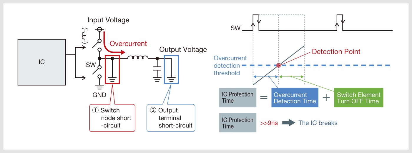
A conventional overcurrent protection operates as follows. First, an overcurrent situation is detected. Next, measures are taken, such as turning OFF the switch element (Fig. 10). Performing these processes takes at least 100ns. Consequently, if the minimum pulse width is 9ns when stable, even if an overcurrent state is detected, protection cannot be provided until the point countermeasures are taken. Meanwhile, the overcurrent conditions will continue worsen, possibly causing damage to the IC itself.

Figure 10. Conventional overcurrent protection function
Overcurrent occurs due to short-circuiting of the switch node or output terminal. Previously, when overcurrent is detected, countermeasures were taken such as turning the switch element OFF. This process takes around 100ns. As a result, if the minimum pulse width is 9ns, even if an overcurrent state is detected, the overcurrent condition will worsen before countermeasures are taken, possibly damaging the IC.
Furthermore... Configuring a conventional overcurrent function requires a dedicated detection element and operation circuit. This unfortunately increases the IC chip area.
Also, when looking at the application scope, a narrow pulse width is more likely to be used for directly converting a high input voltage to a low output voltage. So we can expect that a relatively high input voltage will be applied. For example, even if the overcurrent detection threshold is 2A, for an input voltage of 48V, the power will be 4x that at 12V. This is enough to damage the DC/DC converter IC when an overcurrent situation occurs.
Anything outside the normal state is considered abnormal
As explained above, conventional overcurrent protection functions cannot be used in DC/DC converter ICs with an ultra-narrow minimum pulse width of 9ns. Therefore, a radical change in thinking is necessary.
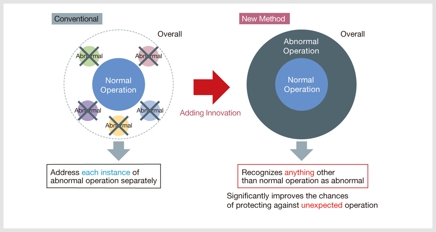
The conventional method can be described as one in which each abnormal state that falls outside the range of normal operation is verified. However, this protection method cannot support a minimum pulse width of 9ns. Therefore, in addition to the conventional circuit, we devised a new protection method that recognizes anything outside the normal operating range as an abnormal condition and immediately takes countermeasures (Fig. 11). The key to this method is how normal operation is defined. Because if we can define normal operation, detecting abnormal conditions becomes easy.

Figure 11. The differences in thinking between the conventional and new protection methods
Conventional detection addresses each abnormal operation separately. ROHM's new detection method defines normal operation then determines any case that falls outside of this as an abnormal state and takes appropriate countermeasures.
So first we considered the normal operation of a DC/DC converter IC. In general, DC/DC converter ICs control the output voltage with a PWM signal. The relationship between the input and output voltages is defined by the following equation.
Input Voltage x (Pulse Width/Cycle) = Output Voltage
DC/DC converter ICs always store the input and output voltage information. And the cycle is known. So the pulse width of the PWM signal is already decided at the stage when the switch element is turned ON. This pulse width is modulated by fluctuations in the input voltage and load, but the modulation width is narrow. This constitutes the normal operation of a DC/DC converter IC.
However, when an abnormal condition occurs this modulation width can become extremely wide or narrow. Therefore, both the pulse width and modulation width are regularly checked, and if either is out of the normal range it is deemed to be an abnormal condition. As shown in the equation above, the pulse width can be thought of as a function of the input voltage. This is because the output voltage and cycle are fixed. The modulation width is determined by the zero cross frequency of the feedback loop (the frequency at which the gain becomes 1). The higher the zero cross frequency the faster the response speed. That is, the modulation width becomes wider. Conversely, the modulation width becomes narrower as the zero cross frequency decreases.
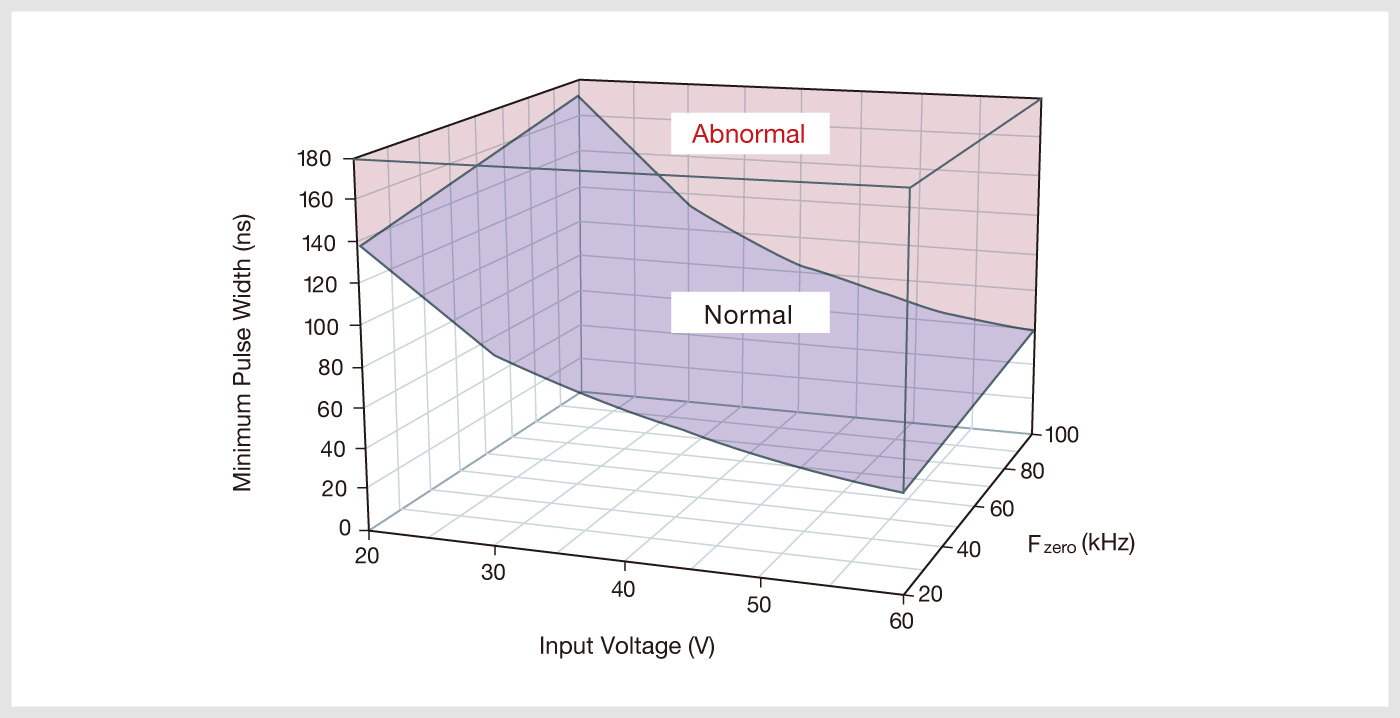
As a result, the pulse width during normal operation can be defined using two parameters: the input voltage and zero cross frequency. This allows us to draw a boundary line between normal and abnormal conditions (Fig. 12). Anything outside the boundary line can be considered abnormal. Judgment is carried out by the PWM control circuit that has the input voltage and zero cross frequency information. Utilizing this method allows for effective use of ultra-narrow pulse widths, enabling fast judgment and making it possible to achieve an overcurrent protection function compatible with DC/DC converter ICs featuring an extremely narrow minimum pulse width of 9ns.

Figure 12. Innovative new overcurrent protection function
Utilizing the two parameters of input voltage and zero cross frequency (Fzero) makes it possible to draw a boundary line between normal and abnormal states.
Aiming for an even narrower pulse
In the future we will strive to achieve even narrower minimum pulse widths. As mentioned earlier, the current limit is 9ns, with a theoretical limit of 6ns. It is actually the material of the switch element itself, silicon, that determines the limit. In the future we will strive to further narrow the pulse width by using GaN (Gallium Nitride). At present, it is not clear exactly how narrow it can get, but it is definitely possible to further narrow the pulse width.
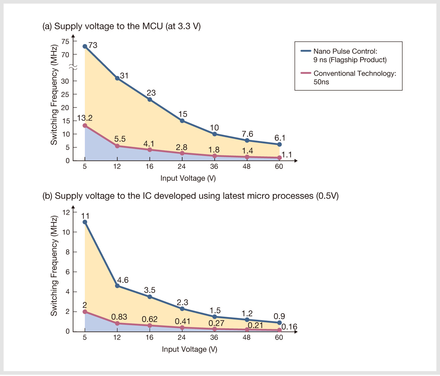
This will make it possible to configure DC/DC converter circuits compatible with larger input-output voltage differences and higher switching frequencies (Fig. 13). Significantly increasing the switching frequency translates to smaller, thinner DC converter circuits. The combination of Nano Pulse Control technology and GaN power devices is expected to significantly advance DC/DC converter technology.

Figure 13. The possibilities of Nano Pulse Control technology
Using an extremely narrow minimum pulse width of 9ns enables configuration of high switching frequency DC/DC converter ICs compatible with large input-output voltage differences. (a) is the supply voltage to the MCU (3.3V), while (b) is the supply voltage to the IC developed using the latest micro processes (0.5V).


