ROHM has developed DC/DC converter control technology featuring an ultra-narrow minimum pulse width of 9ns. Referred to as Nano Pulse Control, this technology enables direct conversion from 48V input to around 1V, even at a high switching frequency of 2MHz. By introducing a ‘flying start’ that obtains the coil current required for control in advance, ROHM was able to successfully reduce the minimum pulse width by two-thirds, from the previous 30ns to 9ns. (This article)
Noise was the source of the problem
Previously, the biggest reason why the minimum pulse width could not be reduced was due to noise generated in the buck DC/DC converter circuits (Fig. 3). Synchronous rectifier buck DC/DC converter circuits utilize 2 switching elements, a high side switch and low side switch, and when one switch turns OFF based on the PWM signal the other switch turns ON. Noise is generated when this switching occurs.

Figure 3. Reasons for noise
Noise (ringing) is generated due to the counter electromotive force of the parasitic inductance component in the wiring. The coil current cannot be detected since the noise is superimposed on the coil current.
The source of this noise is the parasitic inductance of the wiring. Both switching elements as well as the coil are connected with wires. When current with a large rate of change (di/dt) flows, the parasitic inductance of the wiring generates a counter-electromotive force that causes ringing (noise). This noise is superimposed on the coil current.
What negative effects are caused by this noise? Before going into detail, we will briefly explain how to control the feedback loop in buck DC/DC converter circuits. Generally, buck DC/DC converter circuits that supply power to digital ICs such as MCUs and FPGAs utilize ‘current mode’ control. This is because high-speed transient load response can be achieved.
In MCUs and FPGAs, to minimize power consumption in electronic equipment, the operating mode is switched in small increments to match the operating state of the device. At this time the output current of the DC/DC converter circuit can fluctuate significantly, temporarily causing a sudden change in the supply voltage. A DC/DC converter circuit with high transient load response can minimize this change in the power supply voltage. Otherwise, a large supply voltage fluctuation can occur that can lead to malfunction as the supply voltage range specified for the MCU or FPGA is exceeded. Due to this, current mode control with fast transient load response is generally used.
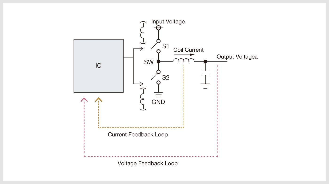
Current mode control utilizes 2 feedback loops (Fig. 4). One loop detects and feeds back the output voltage while the other loop detects and feeds back the coil current.

Figure 4. Current mode control method
Comprised of 2 feedback loops. One that detects and feeds back the output voltage and one that detects and feeds back the coil current.
These two feedback loops are connected. The first loop inputs the detected output voltage to an error amp and compares it with the reference voltage in order to generate a differential voltage. After this, the second feedback loop compares this differential voltage to the coil current that has been converted into voltage to determine the PWM signal pulse width and stabilize the output voltage.
Mask period + circuit delay
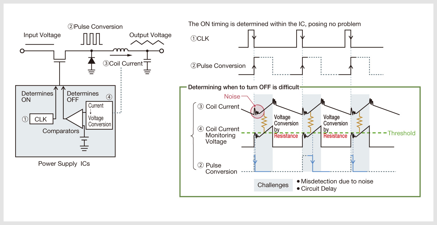
With current mode control it is necessary to continuously detect the coil current. Normally, a current detection resistor is used to convert the coil current to a voltage value so it can be detected. This voltage value is then compared to the differential voltage to determine the timing for turning OFF the PWM signal (Fig. 5). As the ON timing is automatically determined by the buck DC/DC converter's internal clock circuit, the coil current information is not needed.

Figure 5. Two reasons why the pulse width could not be narrowed
One was to avoid noise by applying a mask. The other was circuit delay.
However, as explained earlier, noise is superimposed on the coil current. If the coil current is detected in this state, the noise will be picked up as well, making it impossible to obtain accurate coil current information. In the worst case scenario, even if the actual coil current is below the threshold value, the superimposed noise may push it above the threshold, causing the PWM signal to turn OFF at unpredictable times. Consequently, stabilizing control of the output voltage cannot be achieved. This noise issue is perhaps the biggest drawback of current mode control, and presents a considerable obstacle facing power supply engineers around the world.
In the past, this problem has been addressed by detecting the coil current during periods the noise is not superimposed, and involves masking the periods where noise generation occurs, then starting current detection immediately after. However, a certain amount of time is required for detecting the coil current. This is what is referred to as circuit delay.
In short, there were 2 main reasons why the minimum pulse width could not be reduced until now (Fig. 6). One was that the coil current detection timing was intentionally delayed to avoid noise. And the other was circuit delay. ROHM’s conventional products featured a delay of 70ns due to noise masking and 50ns of circuit delay, resulting in a minimum pulse width of 120ns.

Figure 6. The ON/OFF timing of the switch element
The timing for turning ON is automatically determined by the IC’s internal clock (CLK). The challenge is determining the OFF timing.


