Rohm Breadcrumb

di_what7
High-Frequency Diodes (PIN Diodes)
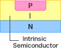
Structure and Features
| Structure | Symbol | Applications・Characteristics |
|---|---|---|
 |
 |
|
A high resistivity I-type semiconductor is utilized to provide significantly lower diode capacitance (Ct). As a result, PIN diodes act as a variable resistor with forward bias, and behave as a capacitor with reverse bias. High frequency characteristics (low capacitance ensures minimal effect of signal lines) make them suitable for use as variable resistor elements in a wide variety of applications, including attenuators, high-frequency signal switching (i.e. mobile phones requiring an antenna), and AGC circuits.
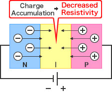
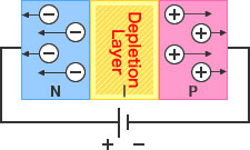
| Forward Voltage | Reverse Voltage |
|---|---|
 |
 |
Variable resistance with forward bias |
Capacitor with reverse biase  |
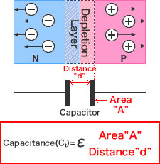
What is the Diode Capacitance (Ct)
The amount of accumulated charge internally when supplying a reverse bias is called the diode capacitance (Ct). An electrically neutral depletion layer is formed by filling the intrinsic layer - created between P and N layers - with charge carriers (holes and electrons). The depletion layer acts as a parasitic capacitor, with a capacitance proportional to the PN junction area and inversely proportional to the distance d. The distance is determined by the concentration of the P and N layers. Supplying a voltage to the diode will increase the depletion layer and decrease Ct.The required Ct will vary depending on the application.
[When supplying a reverse voltage]
Key Points
- The wider the depletion layer (and greater the distance) the lower the capacitance Ct.

electronics_tips_menu