Rohm Breadcrumb

tr_what3
Transistor <Understanding Transistors>
Reverse Current When ON
In an NPN transistor, the Base is at a positive bias, the Collector at a negative bias, and reverse current flows from the Emitter to the Collector. Also, please consider problems that may arise from usage as transistors (such as smaller current gain).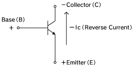
1.It has been determined that no problems, such as degradation or destruction, will arise from use.
2.In the case of an NPN transistor, B is symmetrical with C, and E with N. Therefore, C and E can be used as a transistor, even when connected in reverse. In this case current will flow from E to C.
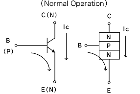
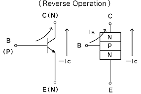
3.The following are characteristics of transistors connected in reverse.
- Low hFE (approx. 10% of the value of the forward direction)
- Low voltage resistance (around 7-8V, about the same as VEBO) The voltage may even be lower (below 5V) in some standard transistors (Please consider that excessively low voltage resistance may result in breakdown and degradation of characteristics)
- VCE(sat) and VBE(ON) should not change much
Package Power Permissible Loss
Package power permissible loss is when voltage is supplied to a transistor and the device begins to generate heat due to power loss due to current flow, particularly when the junction temperature Tj reaches the absolute maximum value (150ºC).
Calculation Method (Where △Tx is the amount of temperature rise when power Px is supplied)
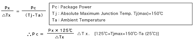
In this case, Pc, Ta, △Tx, and Px can be directly derived from measurement results. Tj is the only value that cannot be directly derived. Therefore, the following shows how to measure VBE, from which we can determine the junction temperature Tj.
In silicon based transistors, VBE will vary based on the temperature.
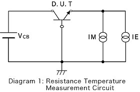
Therefore, the junction temperature can be inferred by measuring VBE. From the measurement circuit shown in Diagram 1, the package power Pc(max) condition is applied to the transistor (In the case of a 1W transistor, the conditions for supply are VCB=10VIE=100mA).
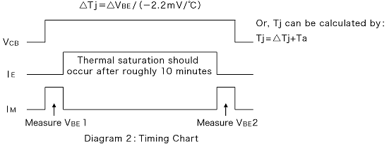
As seen in Diagram 2:
- VBE1 is measured as the initial value of VBE
- When power is supplied to the transistor, heat saturation will occur at the junction
- he value of VBE after will be VBE2
From these results: △VBE=VBE2-VBE1
Here, a silicon transistor will have a fixed temperature coefficient which is approximately -2.2mV/ºC. (NoteL Darlington transistors are due to the use of two transistors -4.4mV/ºC). Therefore, △VBE from the supplied power can be derived from the rise in junction temperature using the following formula.
fT: Gain Bandwidth, Cutoff Frequency
fT: Gain bandwidth indicates the maximum operating frequency of the transistor. At this time the collector current ratio with the base current is limited to 1 (hFE=1).
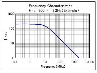
As the frequency of the signal input applied to the base approaches the operating frequency, the hFE begins to reduce. When hFE becomes 1, the operating frequency fT is referred to as the gain bandwidth. fT signifies the operating frequency limit. However, in actuality for operation the value will be about 1/5th to 1/10th that of fT.
f: Depends on the measurement equipment. Reference frequency for measurement.
VCE: optional setting - standard value is normally used for ROHM products.
Ic: optional setting - standard value is normally used for ROHM products.

In addition to low voltage drive MOSFETs for portable products and digital transistors with built-in resistor, ROHM offers a range of transistor products, including standard MOSFETs, bipolar transistors, and complex transistors with integrated diode.
electronics_tips_menu