Rohm Breadcrumb

ad_what3(A/D Converter Configuration 1)
ADC <Basic A/D Converter Configurations>
Numerous configurations exist for ADC (A/D converter). We cover the basic configurations below.
Flash Method
This type of A/D converter utilizes 2N-1 comparators (for an N bit converter) to compare the analog signal with successive reference voltages. The results are then converted into digital format using an encoder.
Features:
- Analog signals are converted into digital signals directly (since the comparators themselves are the sampling devices), making a Sample and Hold circuit unnecessary.
- This allows for extremely fast conversion (with sampling frequencies above 1GHz possible).
- However, the relatively larger size and power consumption (due to the number of comparators are required: 2N-1) limit resolution to around 8bits.

Pipeline Method
In the case of a 1.5bit/stage configuration, the following processes are repeated in order from Stage 1 that determines MSB via pipeline operation (VREF: Reference Voltage).
- Analog input is sampled (using an S&H circuit)
- At the same time the analog input is converted by an A/D converter into a 3-value digital format (1.5bit). (Here the digital output stage is defined.)
- Analog input ≦ -VREF/4 → D="00"
- -VREF/4 < Analog input ≦ +VREF/4 → D="01"
- +VREF/4 < Analog input →D="10"
- These digital values are then converted into analog values using a digital to analog converter (DAC).
- D="00" → DAC output:-VREF/2
- D="01" → DAC output:0
- D="10" → DAC output:+VREF/2
- The negative DAC output voltage is amplified (x2) and output to the next stage.
Once processing of Stage N that determines LSB is completed, the delay between each stage is corrected then digital conversion completed by adding the respective digital output.
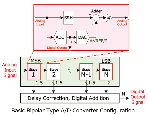
Characteristics:
- High resolution enabled (up to 16bit)
- High-speed conversion possible (200MHz max. sampling frequency)
- There is a necessary wait time until the digital signal is output (based on bipolar operation), making this impractical for applications requiring real-time processing (i.e. control).
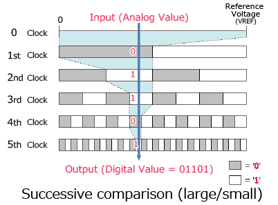
Approximation Method
This method compares the sampled analog input with the converter's output in succession, starting with the MSB.
- The analog input signal is sampled (S&H)
- A successive approximation register (SAR), which is designed to supply an approximate digital code to the internal DAC, is initialized so that the most significant bit (MSB) is set to '1'.
- The digital values from the SAR are converted into equivalent analog values by the internal DAC.
- The sampled input voltage is compared with the DAC output voltage.
- If the sampled voltage > DAC output voltage → MSB = 1
- If the sampled voltage < DAC output voltage → MSB = 0
The digital conversion is completed by repeating the operation up to LSB.
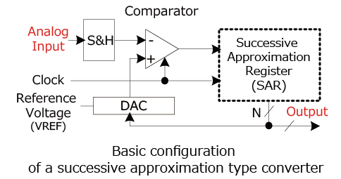
Characteristics:
- High resolution conversion possible (up to 18bit)
- Since a clock cycle is required (resolution + α), conversion speed is moderate (10MHz max. sampling frequency)
- Good response. Connecting a multiplexer to the the input makes it easy to switch analog signals.
ΔΣ Method
After oversampling of an analog signal is performed and converted into low-bit data (i.e. 1bit) corresponding to the amplitude of the analog signal using ΔΣ modulation, conversion into a digital signal at the original sampling rate is completed by filtering the data and removing out-of-band noise using a digital filter.
Oversampling
Quantization error is decreased by sampling at a higher frequency than the original sampling frequency.
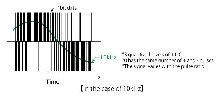
ΔΣ Modulation
The difference (Δ) between the DA converter output voltage and sampled voltage (via oversampling) is integrated (Σ) by the integrator. This integrated value is then converted to low-bit data by comparing with a reference voltage using a comparator.
Delaying the output data by one sampling operation and feeding it back to the input allows modulation to be carried out so that the quantization error generated by the comparator is smaller in the low frequency range and larger in the high frequency range.
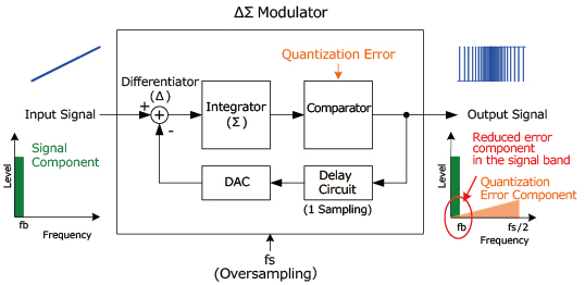
Low-bit data output from the ΔΣ modulator has a large quantization error component in the high-frequency region in addition to the original signal component. However, since these components are separated in frequency and only the quantization error component can be removed by the digital filter, high resolution not possible with other methods can be achieved.
Characteristics:
- Highest resolution among basic A/D converter types (up to 32bits)
- Generally, the conversion speed is slower than successive approximation types.
- Poor response makes it unsuitable for applications that connect a multiplexer to the input for switching analog signals at high speeds.
electronics_tips_menu