Rohm Breadcrumb

tr_what6
How to select
<Selecting Transistors to Ensure Safe Operation>
When a transistor is in operation it experiences electric and thermal loads. The life of a transistor will be short if such loads exceed the maximum tolerances which may break the transistor in a worst case scenario. To avoid this, it is highly recommended to check if there are any issues with the driving the transistor during the design stage.
In this section, we will explain the method of judging whether a selected transistor can be used or not. Please go through this material carefully to avoid potential issues, and to learn how to use transistors safely.
Before Judgement : From Selection to Mounting
Selection of Transistor
You can search for the transistor on our web & short form catalogue.
Get Samples and Data-Sheets
Samples can be purchased from ROHM's Website. Availability of samples for net purchase are constantly expanding.
Mount a Transistor on the Evaluation Board or Function Check
Check Points:

- Make sure that the chosen transistor works safely on the actual circuit.
- Check if the chosen transistor is stable (i.e. functioning for a long period of time ensures reliability)
- Margin of error in the final circuit does not impede the circuit
Judgement : Usable or Not
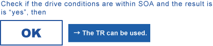
Judgement as to whether it is OK to use a selected transistor or not shall be done based on the following steps.
 |
||||
 |
||||
 |
 |
 |
||
 |
||||
 |
||||
 |
||||
 |
||||
 |
||||
 |
 |
 |
||
 |
 |
|||
 |
||||
 |
||||
 |
||||
Measuring the Actual Current & Voltage Waveform
Confirmation of Current and Voltage
First, check to see what the current and the voltage applied to a transistor is with an oscilloscope. The listed ratings on the datasheets need to match the measured values, the parameters listed below should be given priority.
Priority items:
| Transister Type | Voltage | Current |
|---|---|---|
| Bipolar Transistor | Collector-Emitter Voltage :Vce | Collector current : Ic |
| Digital Transistor | Output voltage :Vo(GND-OUT) | Output current:Io |
| MOSFET | Drain-Source Voltage : Vds | Dorain current : Id |
Example: Waveform When Switching 2SD2673(100μs / div)
Is the Absolute Maximum Rating Observed all the Time?
Confirmation of Absolute Maximum Rating
Check if the current and the voltage(Confirmation of current and voltage)are not exceeding the absolute maximum rating stipulated in the data sheet. There are items not checked in the table above, but all such unchecked items also need to stay below the absolute maximum rating.
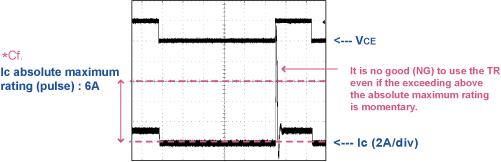
A transistor cannot be chosen if the peak current or the voltage surge could go beyond the absolute maximum rating range even for a moment. Otherwise, there is the possibility of performance deterioration and destruction of a device if driven beyond the absolute maximum.
Example: Data sheet of 2SD2673 (Description of Absolute Maximum Rating)
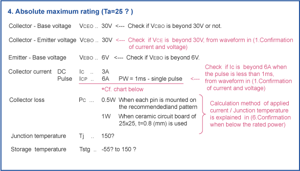
Example: A Case Where the Absolute Maximum Rating is Violated Momentarily (NG)
Is the Use of a Transistor Within SOA?
Confirmation of Safe Operating Area (SOA*) Part 1
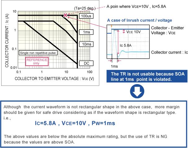
SOA specifies the area where a transistor can be driven safely. However, SOA is merely based on a single (One) pulse alone. Therefore, it is necessary also to check if all the pulses stay within SOA if the transistor is driven by repetitive pulses, and also the averaged applied current to be calculated in (Confirmation of Safety Operation Area (SOA) - Part 2) stays within the rated power.
*1 Also called ASO (Area of Safe Operating).
SOA Compliance Check
Check if waveform confirmed in the 1.Confirmation of current and voltage stays within SOA. NG (Transistor Not Usable) judgement must be concluded if inrush / peak current or voltage surge goes beyond the absolute maximum rating even for a moment.
Also, please double check that SOA has not been violated, even if the waveform in the Confirmation of absolute maximum ratingis within the absolute maximum rating, it's better to be safe than sorry. (See the example below.)
Example : 2SD273 SAFETY OPERATING AREA
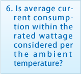
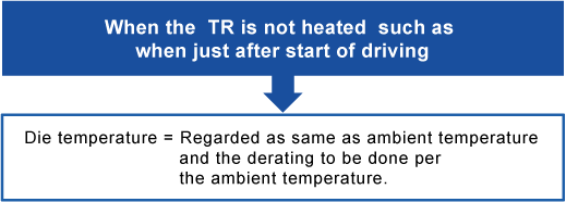
Is the use of TR within SOA derated per the ambient temperature*1?
*1 The ambient temperature where the TR is used or the temperature of die when the temperature of the TR is elevated by its heat.
Confirmation of Safety Operation Area (SOA) Part 2
Normally, SOA is defined by room temperature (25 deg).
Ways to Reflect Derating into SOA Graph:
・Bipolar TR / DIgital TR
・MOSFET
*The temperature requiring derating is basically corresponds to the temperature of die.
Please refer to "Calculation method of die temperature"which is prepared separately for details of die temperature calculation.
Temperature Derating Method of SOA
SOA (Safe Operating Area)
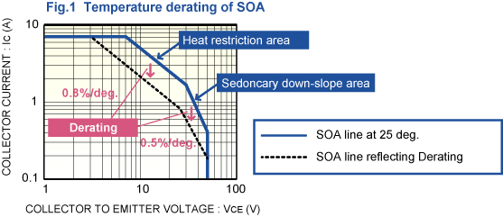
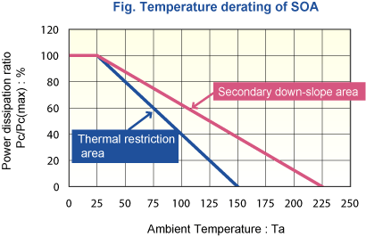
SOA (Safe Operating Area) needs temperature derating when the ambient temperature is more than 25 deg. or the temperature of die is elevated by the heating of the transistor itself. Temperature of derating is the ambient temperature for the former, and the die temperature for the latter. To be specific, the SOA line needs to be shifted toward the direction where the current is smaller. The derating ratio varies depending on the area as per the Fig.1
Heat-Restriction Area
In this area, SOA line has a 45° downward inclination. (Power constant line)In this area, the derating ratio is 0.8% / deg.
Secondary Down-Slope Area
For transistors, there is secondary down-slope area due to thermal overdrive. SOA in this area has the slope is more than at 45°and the derating ratio is 0.5% /deg.
Example Ta=100 deg.
2-1. Derating in the area of heat-restriction area In case of ambient temperature of 100 deg.
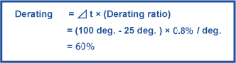
Therefore, the judgement should be made by considering SOA line shift by 60% toward the smaller current direction.
Derating in the Area of Secondary Down-Slope
Likewise as above, the calculation is done as below.
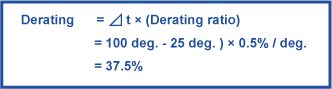
Accordingly, the judgement should be made by considering SOA line shift by 37.5% toward the smaller current direction.
Continuous pulse? Single pulse?
Single Pulse
A sudden inrush of current (from power being applied for example) is called a single pulse
Continuous Pulse
Unlike single pulse, it is called "continuous pulse" if the pulses are loaded repeatedly. In that case, check if
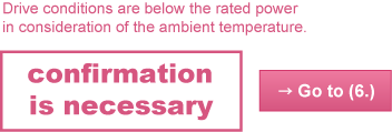
Is Averaged Power Consumption Below the Rated Power at the Ambient Temperature?
Confirmation When Below the Rated Power
Below the rated power under the ambient temperature = Die temperature below the maximum rating 150 deg.The rated power is decided as the power which heats up the die at 150 deg.
(For details, please refer to the Calculation method of die temperature prepared separately.
Power Calculation Method
In principle, the averaged power is the value obtained as a result of dividing the integration of Current and Voltage by the time. i.e.,
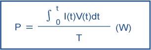
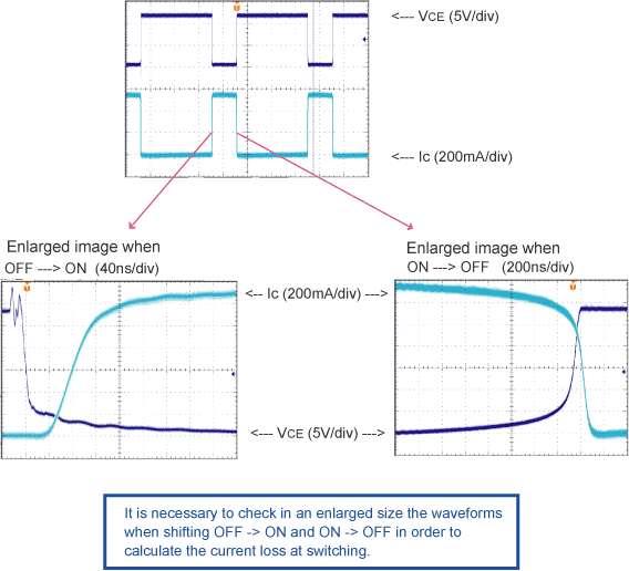
Now, thinking the following switching behavior for instance.
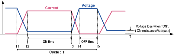
In this case, the calculation should be done by dividing one cycle in four.
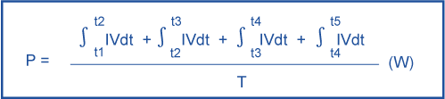
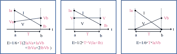
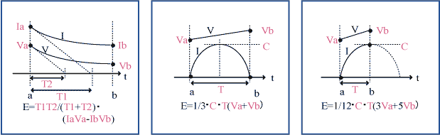
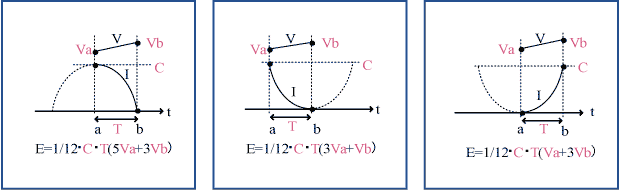
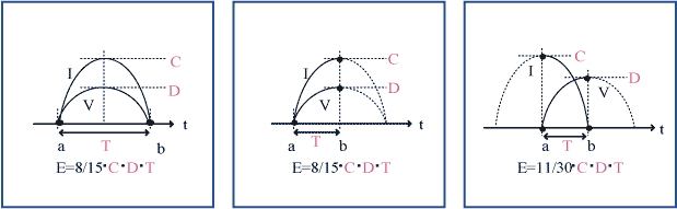
In actual integration calculation, please refer to "Integration Formula" prepared separately.
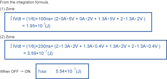
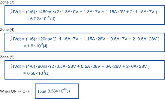
Let's make calculation for the waveform observed in(1.Confirmation of current and voltage) as an example.
When OFF ---> ON
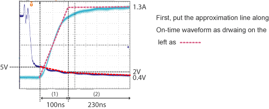
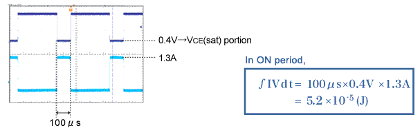
ONperiod
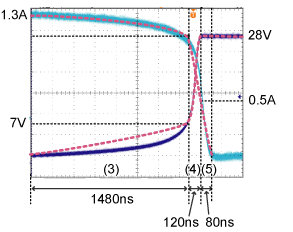
When ON ---> OFF
When There is Almost No Current When OFF
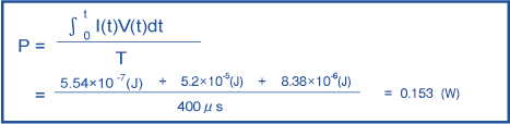
There should be some nA to 10nA level of leak current should exist in reality, and the current consumption as 0 (zero) while OFF state. From the above calculation, if we divide all the total of integration result per each zone by 400μs which is the length of cycle, the the averaged current consumption is figured out as
We took an example of bipolar transistor 2SD2673 earlier in order to do integration calculation of collector current Ic and Collector-Emitter voltage Vce. The integration calculation in case of other TR types can be as below for obtaining the averaged current consumption.
- Digital TR : Output Current Io and Outpout Voltage Vo
- MOSFET : Drain Current Id and Drain-Source Voltage Vds
After getting the averaged current consumption, we should check with Pc (Collector-loss) for digital TR (Drain-loss for MOSFET).
Example : Data Sheet of 2SD2673
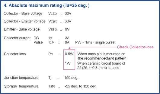
In this case, the averaged applied power is 0.153W and Collector-loss is 0.5W (Recommended land : glass epoxy circuit board), so that the use of this TR under the ambient temperature of 25 deg. is OK. (In the strict sense, Pc should differ depending on the difference of heat dissipation conditions as from the types of circuit board or as from land-pattern area. However, we assume that the the recommended lnd-patterns are employed.)
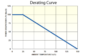
When the ambient temperature is above 25 deg., please consider the temperature derating in designing per the derating curve.
For the details of Die Temperature Calculation, please refer to the separate documents "Calculation method of die temperature".
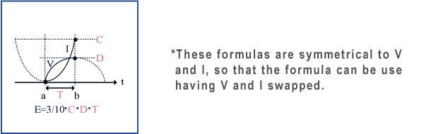
Power Calculation Integration Formula
Calculation of power between a - b by integration with Current I and Voltage V.

electronics_tips_menu