Rohm Breadcrumb

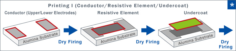
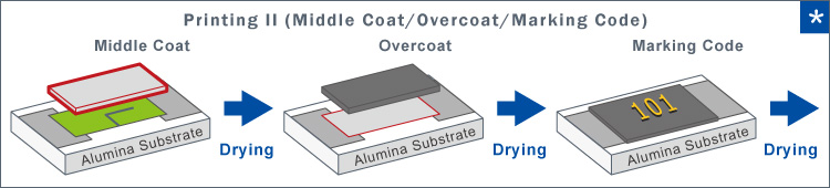
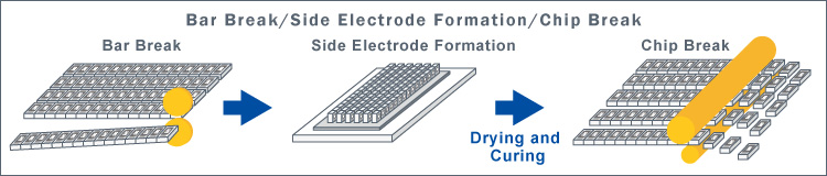
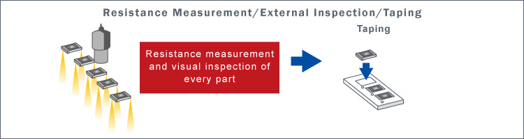
Resistor manufacturing flow example
SMD Resistor
<Chip Resistor Structure>
Resistor Manufacturing Flow Example
The following illustrates the manufacturing flow of a typical SMD Resistor (MCR Series).

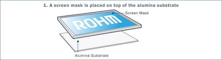
In actuality the entire alumina substrate is processed at one time, but for illustrative purposes only one chip will be shown.


What is Screen Printing?
Each layer of a ROHM chip resistor is formed by screen printing. Screen printing involves creating a print pattern on the mesh surface of a screen mask, then applying paste, then transferring the pattern onto a target object (alumina substrate) by scraping the paste with a squeegee.
Screen Printing Flow


Laser trimming
The Need for a Laser Trimming Process
Screen printing is used to form each layer of a thick film chip resistor and involves placing paste on the alumina substrate. Hundreds of chips are processed at the same time, inevitably leading to slight variations in printing conditions (i.e. paste thickness).
This results in varying resistance values, making it impossible to ensure optimum resistances. Therefore, an additional process is required to adjust the resistance values to within specified tolerances.


The Laser Trimming Process
A laser cuts the resistive element while the resistance is measured in order to achieve target resistance values with minimal variation. Laser trimming narrows the current pathway, which increases resistance. Once the target resistance has been met the laser is stopped to reduce variations between chips.


electronics_tips_menu