Rohm Breadcrumb

tr_what5
MOSFET
<Understanding MOSFET Characteristics>
MOSFET Parasitic Capacitance and Temperature Characteristics
Parasitic Capacitance
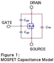
Parasitic capacitance exists in power MOSFETs as shown in Figure 1.
Sometimes known as stray capacitance, parasitic capacitance is unavoidable and typically unwanted that exists between the parts of an electronic component or circuit simply because of how close they are to one another. Capacitance is the ability of a system to store an electric charge.
The Gate terminal in a MOSFET is isolated from the other terminals by an oxide film. The silicon under the gate has the opposite polarity to the drain and source which results in the formation of PN junctions (diode) between the Gate, Drain and Source regions. Cgs and Cgd are the capacitances of the oxide layers, while Cds is determined by the junction capacitance of the internal diode.
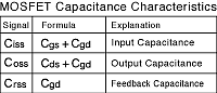
Generally, all 3 capacitances (Ciss,Coss,Crss) listed in Table 1 are included in MOSFET specifications.
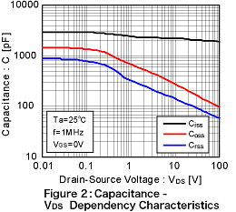
As shown in Figure 2 the capacitance characteristics may depend on VDS (Drain-Source voltage). As VDS increases the capacitance decreases.
Temperature Characteristics
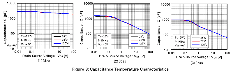
There are almost no differences in the capacitance characteristics at different temperatures. Temperature measurement examples are shown in Figure 3 (1)-(3).
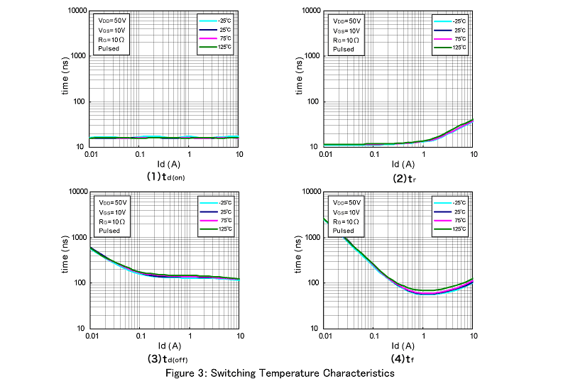
MOSFET Switching and Temperature Characteristics
What is MOSFET Switching Time?
The MOSFET will turn ON or OFF after the Gate voltage turns ON/OFF. The time in between turning ON or OFF is called the switching time. Various switching times are listed in Table 1 below. Generally, td(on) , tF , td(off) and tr are specified. ROHM determines the typical values utilizing a measurement circuit like the one shown in Figure 2.
Temperature Characteristics
The switching time is only slightly affected by temperature rise - on the order of 10% at 100°C. In other words, switching characteristics are largely independent of temperature. Measurement examples are shown in Figure 3 (1)-(4).
VGS threshold: VGS(th)
VGS(th) is the voltage required between the Gate and Source to turn ON the MOSFET.In other words, supplying a voltage greater than VGS(th) will turn ON the MOSFET.
To determine the amount of current that flows through the MOSFET when ON it is necessary to refer to the specifications and electrical characteristics for each element.
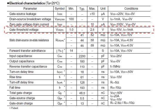
Table 1 lists the relevant electrical characteristics. In the case of VDS=10V a threshold voltage of between 1.0V and 2.5V is required for an ID of 1mA.
Table 1: Electrical Characteristics
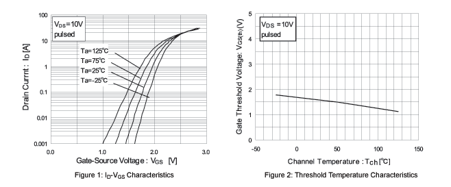
ID-VGS and Temperature Characteristics
ID-VGS and threshold temperature characteristics examples are shown in Figures 1 and 2 above. As seen in Figure 1, a large Gate voltage is required for large current flow.
Although the models listed in Table 1 feature a threshold value less than 2.5V, 4V drive is recommended. Always make sure there is a sufficient Gate voltage to turn the MOSFET ON.
Referring back to Figure 2 we see that the threshold value decreases in proportion with the temperature. Therefore, the element channel temperature can be calculated by monitoring the change in threshold voltage.

ROHM's MOSFET has the wide drive types and supports from a small signal to high power. In addition, be superior to high-speed switching and low On-Resistance, and ROHM's MOSFET is available by wide application.
electronics_tips_menu