Rohm Breadcrumb

SiC SBDの特徴(what2)
Silicon Carbide
<Types of SiC Power Devices>
SiC SBD Device Structure and Features
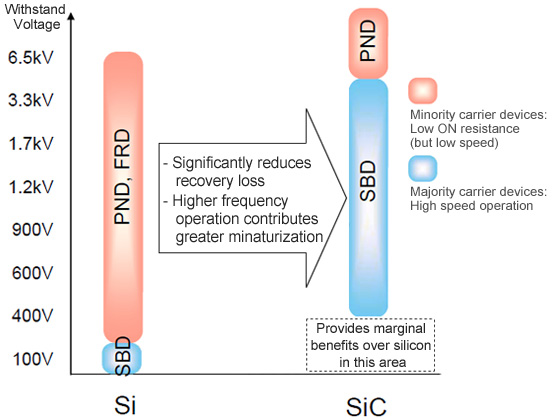
Incorporating Silicon Carbide high-speed device construction into Schottky barrier diodes (SBDs) makes it possible to achieve withstand voltages greater than 600V (in contrast to ~200V with silicon SBDs).
As a result, replacing existing mainstream PN junction diodes (fast recovery types) significantly reduces recovery loss, contributing to lower noise and greater compactness in passive components, such as coils. This is due to increased power supply efficiency and higher frequency operation. This ensures support for power factor correction circuits (PFCs) and rectifier bridges, making them suitable for a wider range of applications, including AC, power supplies, solar power conditioners, EV rapid chargers.
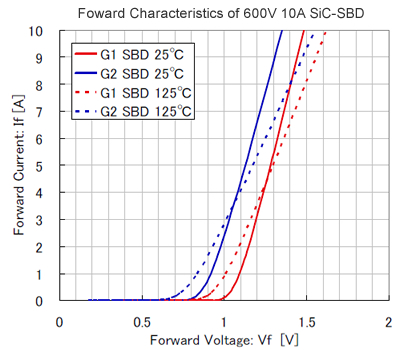
SiC SBD Forward Characteristics
The rise voltage of SiC SBDs is less than 1V - equivalent to that of FRDs. Rise voltage is determined by the height of the Schottky barrier. However, although designing a lower normal barrier height makes it possible to reduce the rise voltage, this comes at the expense of leakage current, which increases during reverse bias. In response, ROHM has successfully devised a process for its 2nd generation SBDs that reduces rise voltage by approx. 0.15V while maintaining leakage current and recovery characteristics equivalent in conventional products.
In addition, temperature dependence differs significantly from Si FRDs, with Vf increasing along with operating resistance at high temperatures. This helps to prevent thermal runaway, ensuring worry-free operation even when connected in parallel.
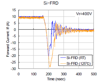
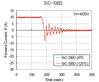
SiC SBD Reverse Recovery Characteristics
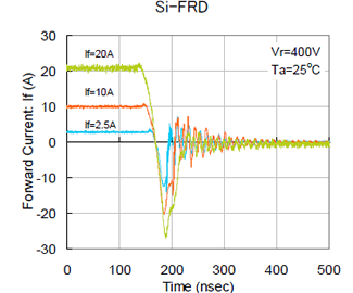
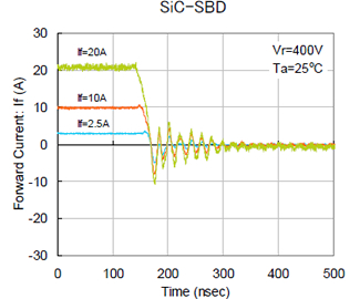
In silicon high-speed PN diodes (FRDs) large transient current flows the moment the direction switches from forward to reverse, which can lead to large losses when shifting to a reverse bias condition during this time. When forward current is applied, minority carriers accumulated in the drift layer contribute to electrical conduction until they disappear (storage time). This increases both recovery time and recovery current as the forward current rises and temperature increases, causing significant loss.
In contrast, SiC SBDs are majority carrier devices (unipolar) that do not use minority carriers for electrical conduction, so in principle minority carrier accumulation does not occur. As a result, only a small amount of current flows for discharging the junction capacitance, achieving considerably less loss than silicon FRDs. This transient current is largely independent of temperature and forward current, making stable high-speed recovery possible under virtually any environment. Reduction of noise that occurs due to reverse recovery current can also be expected.
Reverce Recovery Waveform (600V 10A)
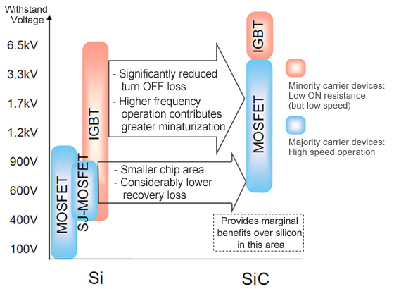
SiC MOSFET Device Structure and Features
With silicon, as the withstand voltage rises the resistance per unit area also increases (by approx. the square to the 2.5th power of the withstand voltage). Consequently, IGBTs (Insulated Gate Bipolar Transistors) are primarily used for voltages above 600V. IGBTs are able to offer lower ON resistances than MOSFETs through conductivity modulation where minority carriers (holes) are injected into the drift layer.
However, this leads to the generation of tail current during turn OFF caused by minority carrier accumulation, resulting in larger switching losses. In contrast, Silicon Carbide features a lower drift layer resistance than silicon devices, eliminating the need for conductivity modulation and enabling high withstand voltage with low resistance when used in high-speed devices such as MOSFETs. Therefore, since in principle no tail current is generated, replacing IGBTs with SiC MOSFETs should reduce switching loss significantly, making it possible to decrease the size of cooling countermeasures.
Silicon Carbide also contributes to smaller passive components through high-frequency operation not possible with conventional IGBT solutions. 600V-900V SiC MOSFETs provide a number of additional advantages, including a smaller chip area (enabling smaller packages) and dramatically lower recovery loss. As a result, application has expanded to power supplies for industrial equipment and inverters/converters for high-efficiency power conditioners.
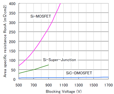
Normalized ON Resistance
SiC offers 10x the dielectric breakdown electric field strength of silicon, making it possible to achieve higher breakdown voltages through lower resistivity and a thinner drift layer. This enables a lower normalized ON resistance (ON resistance per unit area) at the same withstand voltage.
For example, at 900V and the same ON resistance chip size can be reduced by 35x vs silicon MOSFETs and 10x compared with SJ MOSFETs. And in addition to delivering low ON resistance in a compact form factor, gate charge Qg and capacitance can be reduced as well.
Typically, SJ MOSFETs are available in withstand voltages only up to 900V. But using SiC allows for voltages over 1700V with low ON resistance. In fact, SiC makes it possible to develop devices that combine low ON resistance, high withstand voltage, and high-speed switching, eliminating the need for bipolar devices such as IGBTs (which provide low ON resistance but with slow switching speeds).
Vd-Id Characteristics
SiC MOSFETs feature no rise voltage like with IGBTs, resulting in low conduction loss throughout the entire current range. In addition, the ON resistance of Si MOSFETS at room temperature increases by 100% at 150C. But with SiC MOSFETs the rate of increase is relatively low, simplifying thermal design while ensuring low ON resistance even at high temperatures.
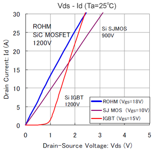
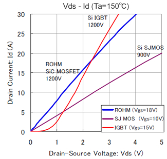
*The data indicates evaluation results conducted by ROHM under the same conditions
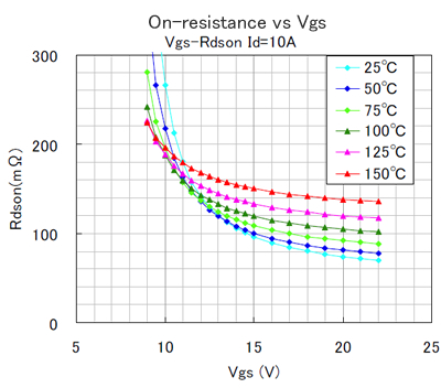
Drive Gate Voltage and ON Resistance
Although SiC MOSFETs feature lower drift resistance than Si MOSFETs, at the current technical level mobility of the MOS channel section is low, resulting in higher MOS channel resistance. This makes it possible to obtain a lower ON resistance at higher gate voltages (gradual saturation at Vgs=20V+).
However, inherent ON-resistance performance cannot be demonstrated at drive voltages used for standard IGBTs and Si MOSFETs (Vgs=10-15V). Therefore, to obtain sufficient ON resistance a drive voltage in the vicinity of Vgs=18V is recommended.
electronics_tips_menu