Rohm Breadcrumb

op_what3(Amplification Factor and Voltage Gain)
Typical Parameters of Opamps
<Amplification Factor and Voltage Gain>
Amplification Factor and Voltage Gain
When a voltage is supplied to the input of the amplifier circuit it is multiplied by the amplification factor and appears at the output. This amplification factor is obtained by dividing the output voltage by the input voltage.
With an input voltage Vs,and output voltage Vo, the amplification factor Av is defined by the following formula.
| AV = | VO | [ Multiplied ] |
| VS |
What is a Decibel (dB)?
The logarithm of the amplification factor (multiplied by 20) is expressed in units of decibels (dB).
For example, for an opamp with an open gain of 100,000x (105x), the decibel notation will be as follows.
| 20log10 (105) = 100 [dB] |
In this way, we can express a large amplification with many multiples of 10 by a smaller number using decibels.
Other units used in analog circuits are shown below.
(a) dB : The logarithm of the ratio of 2 quantities, multiplied by either 10 or 20.
| [dB] = 10log | P1 | (Power) | |
| P2 |
| [dB] = 20log | V1 | (Voltage) | |
| V2 |
(b) VP-P : Difference between the minimum and maximum values of the waveform.
(c) Vrms : Obtained by taking the square root of the mean average of the square of the voltage.
- 1Vrms = 2√2
(d) dBV : Representation based on 1Vrms
- 0dBV = 1Vrms
(e) dBm : A reference voltage that gives rise to a power of 1mW for a given load.
Typical load values include 50Ω and 600Ω.
- 0dBm=0.224Vrms (With a 50Ω load)
- 0dBm=0.775Vrms (With a 600Ω load)
(f) oct (octave) : 1oct is twice the value for a given frequency.
-6dB/oct indicates that there's a drop of 6db if the frequency is doubled.
(g) dec (decade): 1dec is 10x the value for a given frequency.
-20dB/dec shows that there's a drop of 20dB if the frequency is increased by 10x.
*From (f) and (g), -6dB/oct= -20dB/dec.
(h) dB (decibel) basic calculation
- 3dB ≒ 1.41x ≒ √2
6dB ≒ 2.00x
10dB ≒ 3.16x
20dB ≒ 10x
Example: 16dB=10dB+6dB → 3.16×2=6.32x
Input Offset Voltage
With an input offset voltage and a differential input circuit, ideal opamps and comparators will have an offset voltage of 0V, including error voltage. When inputting a common-mode (same) voltage to the input pins of an opamp or comparator, with an ideal opamp no output voltage will be output, but in the case where an input offset voltage exists, a voltage will be output based on the input offset voltage. This input offset voltage, which is the differential voltage required to make the output voltage 0V, becomes the input conversion value.
The benefit of expressing in terms of input conversion is that utilizing input conversion voltage makes it easy to estimate the effects on the output voltage, even with opamps and comparators featuring different amplification rates and circuit configurations. Offset voltage is normally expressed in units of mV or µV.
Values closer to 0 are more ideal.
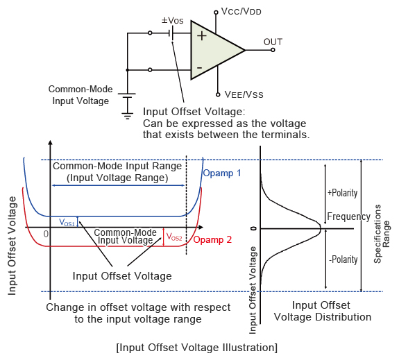
The offset voltage increases rapidly when its out of the common-mode input range, and in this region opamps and comparators cannot operate. In addition, if we observe the frequency occurrence of the offset voltage, we will see that the normal distribution will center around 0V.
In other words, it will be stochastically distributed within the defined range. Normally, since the representation of the standard value is described as an absolute value, both + and - offset voltages exist.
Slew Rate (SR)
The slew rate is a parameter that describes the operating speed of an opamp. It represents the rate that can change per unit time stipulated by the output voltage. For example, 1V/us indicates that the voltage can change by 1V in 1us. Ideal opamps make it possible to faithfully output an output signal for any input signal. However, in reality slew rate limits do exist.
When supplying a rectangular pulse at the input with a steep rise and fall, this indicates the possible degree of change in the output voltage per unit time.
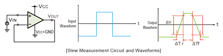
The rise and fall slew rates are calculated by the following equations:
| SRr= | ΔV | SRf= | ΔV | |
| ΔTr | ΔTf |
The slew rate is stipulated based on the slower of 'rise' and 'fall'. In other words, it signifies the maximum value of the slope of the output signal. For signals with steeper changes (slopes), the output will become distorted and cannot follow. And even when configuring an amplifier circuit, since the slew rate is the ratio of output change, no change will occur.
Opamps are used to amplify both AC and DC signals. However, opamps have limited response speed, and therefore cannot handle all types of signals. In the above diagram [Slew Measurement Circuit and Waveforms] of a voltage follower circuit, the input and output voltage ranges are restricted by the DC input voltage. In addition, AC signals with a frequency component are constrained by the slew rate and gain bandwidth product.
Here, we consider the relationship between the amplitude and frequency, or slew rate. The opamp determines the maximum frequency that can be output.
Calculate the slew rate required to output the waveform shown at right.
y=Asinωt
The slew rate is the slope of the tangent of the sine wave, differentiating the above equation.
| dy | =Aωcosωt | ωt=0 | |
| dt |
The slew rate is
SR=Aω ω=2πf
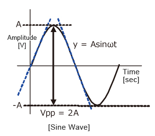
Furthermore, since the amplitude of the sine wave becomes Vpp=2A (peak-to-peak), the equation can be modified as follows.
| f = | SR | = | SR | [Hz] | VPP = | SR | [V] | |
| 2π × A | π VPP | π f |
This frequency(f) is referred to as the full power bandwidth. These are conditions where the amplification factor in the opamp has not been set, in other words the relationship of the frequency and amplitude (within the output voltage range) that can be output by the opamp in a voltage follower circuit.
Example:
The frequency capable of outputting a 1Vpp signal in an opamp where SR=1V/us is:
| f = | SR | = | 1 | × | 1 | = 318.4kHz |
| π VPP | 10-6 | π × 1 |
When exceeding the frequency calculated above (with a constant amplitude), the waveform is limited by the slew rate and the sine wave will become distorted and become a triangular wave.
Negative Feedback System
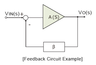
Although opamps are high voltage gain amplifiers, virtually no opamps carry out standalone amplification. This is because it is difficult to control the open gain variations and narrow-band amplification factor. Therefore, a negative feedback circuit is typically used.
The diagram at right shows an example of a negative feedback system.
Advantages of Negative Feedback Circuits:
- Widens the Region (Bandwidth) Where the Gain of the Amplifier Circuit Becomes Constant
- Minimizes the effects of opamp open gain variation
- Suppresses distortion
Widens the Region (Bandwidth) Where the Gain of the Amplifier Circuit Becomes Constant
First off, determine the transfer function, which relates the output to the input of the model.
| VO(s) | = | A(s) |
| VIN(s) | 1 + βA(s) |
AO : Opamp Open Gain (Open Loop Gain)
β : Feedback Factor
1+βA(s) : Amount of Feedback
Loop Gain : βA(s)
In addition, as shown by the following equation, the opamp has a transfer function for 1st order lag
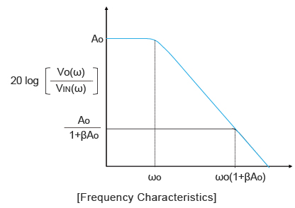
| A(s) | = | AO | |
| 1 + | ω | ||
| ωO | |||

| VO(s) | = | AO | × | 1 | |
| VIN(s) | 1 + βAO | 1 + | ω | ||
| ωO(1 + βAO) | |||||
The above frequency characteristics illustrate the relationship of the formula above.
Applying negative feedback will reduce the gain and amount of feedback, showing that ωO will expand to ωO(1+βAO).
Minimizes the Effects of Opamp Open Gain Variation
Next, assuming that the open gain of the opamp in the transfer function equation (relating the output to the input) is sufficiently large (AO>>1), the gain of the negative feedback circuit at low frequencies can be approximated to 1/β.
In other words, when the open gain of the opamp is large, the gain of the feedback circuit is determined solely by the feedback ratio (regardless of the gain).
As a result, the amplification factor of the amplifier circuit (i.e. inverting amplifiers) at low frequencies is solely determined by the external resistance.
Also, in the case the open gain is sufficiently large (AO>>1), the effects of open gain (based on temperature characteristics and production variations) is small, even with some fluctuations.
| VO | = | AO | = | 1 | ≒ | 1 | |
| VIN | 1 + βAO | 1 | + β | β | |||
| AO | |||||||
Suppresses Distortion
A feedback circuit with error elements is shown in the figure below. Here the error elements generated by the opamp are VD.
Elements such as distortion, error voltage, and noise are included.
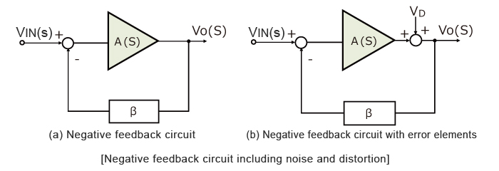
| VO(s) = | A(s) | VIN(s) + | A(s) | VD | |
| 1 + βA(s) | 1 + βA(s) |
The transfer function including distortion is shown at the equation at right. As shown here, as the gain increases VD becomes smaller, and we can see that the error is mitigated.
Drawbacks of Configuring a Negative Feedback Circuit:
- Lower amplification factor compared with open gain
- Feedback may cause the circuit to oscillate
electronics_tips_menu