Rohm Breadcrumb

tr_what4
Digital Transistor
<Understanding the Principles of Digital Transistors>
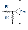
Selection Method
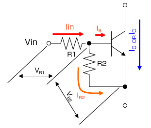
1) The IC/IB ratio needed in order to saturate the transistor is 20/1
2) Input resistor R1: ±30%, E-B resistor R2: R2/R1=±20%
3) VBE: 0.55V to 0.75V
Equations Used for Digital Transistors
- The relationship of the DC current gain of digital transistors
GI: Digital transistor DC current gain
 GI=Io/Iin
hfe=Ic/IB
Io= Ic , Iin= IB +IR2, IB=IC/hfe , IR2=VBE/R2
Voltage relationship: Vin=VR1+VBE
- The relationship with collector current:

∴ Ic= hfe×((Vin-VBE)/R1 )- (VBE/R2 )) ・・・(1)
The value of hfe mentioned here is not saturated at VCE=5V/IC=1mA.
When using as a switch the current ratio for saturationIC/IB=20/1 is required.
∴ Ic= 20×((Vin-VBE)/R1 )- (VBE/R2 ))・・・(2)
Replace the hfe in (1) with 20/1.
Calculations are carried out taking into account variations.
The worst-case values for R1 (+30% max.), R2 (-20% min.), and VBE (0.75V max) are utilized in equation (2). Select R1 and R2 of the digital transistor from the below equation in order to exceed the output current Iomax.
∴ Iomax≦20((Vin-0.75)/(1.3XR1)-0.75/(1.04XR2))
Digital Transistor Part Number Explanation

The Difference Between Io and Ic
Ic: The maximum theoretical current that can flow through a transistor
Io: The maximum current that can be used for a digital transistor
Notes
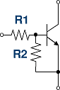
The DTA/C series of digital transistors support 100mA of current flow. For these products, Ic is defined as 100mA. Connecting resistors R1 and R2 makes it a digital transistor. Ic=100mA operation requires a high input voltage Vin to ensure sufficient base current IB.
However, the maximum input voltage Vin(max) is defined by the power tolerance (package power) of the input resistor R1, which is determined on the absolute maximum ratings. Therefore, since this rating may be exceeded when Ic=100mA, Io is defined as the current value that can flow through the digital transistors without exceeding Vin(max).
As you may know, the absolute maximum ratings stipulate that 2 or more parameters cannot be simultaneously supplied, so there is no problem with a notation using only Ic. However, Io may also be listed in accordance with actual usage conditions.
From the above, after taking into account circuit design, Io can be considered the absolute maximum rating.
The difference between GI and hFE
hFE: DC current gain in general transistors
GI: DC current gain in digital transistors
Notes
GI and hFE both represent DC current gain in common-emitter configurations. Digital transistors are conventional transistors that incorporate 2 internal resistors.
Here since the DC current gain = output current/input current the gain is not reduced by the input resistor R1. Therefore, for types that integrate only an input resistor R1, gain is represented by hFE, and will be equivalent to the hFE of the configured transistor.
However, when connecting a resistor (R2) between the emitter and base, the input current is diverted away from the base and safely directed to the emitter. As a result, amplification is reduced. This value is represented as GI.
The Difference Between VI(on) and VI(off)
It is easy to mistakeVI(on) with VI(off) and vice versa.
VI(on): The minimum voltage required to turn the transistor ON.
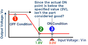
Common misunderstanding:
 : The input voltage increases constantly from 0V
 : After a short time the voltage will reach 1.8V, turning the digital transistor ON
 : Since this voltage is below the 3V listed in the specifications, it is considered no good.
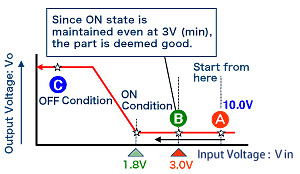
Actual operation:
 : First, increase the input voltage Vin to a level sufficient to turn ON the transistor (i.e. 10V)
 : Gradually lower the voltage to the level noted in the specifications (i.e. 3V). If the transistor remains ON it is considered good.
 : Continue to decrease the voltage supplied to the base until the transistor turns OFF. Since this point is below 3V, the transistor works.
Digital Transistor Temperature Characteristics
VBE, hFE, R1, and R1 will vary depending on the ambient temperature.
hFE will change by: 0.5%/ºC (approx.)
BE will vary by around -2mV/ºC (within the range of -1.8 to -2.4mV/ºC)
R1 will change based on the graph below. 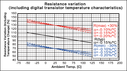
Output Voltage - Output Current Characteristics in the Low-Current Region
The output voltage-output current characteristics of digital transistors are measured using the following method.
FFor DTC114EKA measurement is performed using Io/Ii=20/1
i=IB+IR2 from (IR2=VBE/10k=0.65V/10k=65uA)
If IB=Ii-IR2=Ii-65uA (if Ii becomes less than 65uA) IB will not flow, and Vo [VCE(sat)] will increase. If this happens Vo cannot be measured in the low current region.
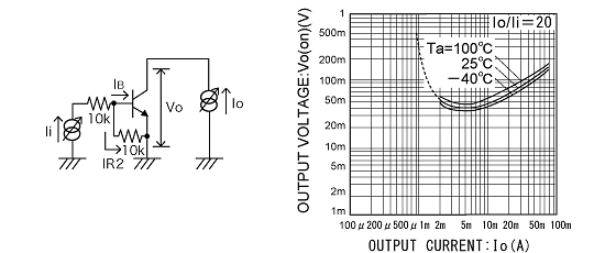
If the input current to the base is too small (for example, it cannot overcome the 65uA in the example above), then no current will flow through the base and thus the transistor will never conduct.This will cause the output voltage Vo (VCE(sat)] to rise in the low current region
Digital Transistor Switching Operation
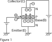
Transistor Operation
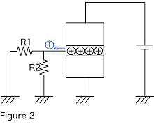
For NPN transistor operation, voltage is supplied as in Diagram 1. In this circuit, the base (B) - emitter (E) region is forward biased which results in current flow through the base. In other words, the base is injected with holes.
When this happens the free electrons in the emitter (E) are drawn towards the base. However, since the base region is extremely narrow, free electrons flow through the base region to the collector due to voltage bias from the collector. Because of this, current flows from the collector to the emitter.

Switching Operation
Transistor operation consists of both amplification and switching. During amplification, Ic, equivalent to hFE times the base current, flows. The output current in the active region can be controlled by adjustment of the input current.
Switching operation ensures saturation conditions while ON (smallest collector-emitter voltage possible). In this saturation region, there is an excessive number of holes, which then exit through the base terminal from the base region. Collector current flows until all of the + holes exit from the base region. The time it takes for this to occur is referred to as tstg (OFF time). The quicker the holes exit the base region the shorter the OFF time.
In digital transistors, R1 and R2 act in series as a path for the holes to exit the base region while the transistor is OFF. R2 should be made as small as possible (with a given fixed R1) in order to minimize OFF time.
Digital Transistor Terminology
- VI(on)min: Minimum Input ON Voltage
Forward voltage Vo applied between the OUT and GND pins - the minimum input voltage required for output current (Io) flow. Or the minimum input voltage needed to turn ON a digital transistor.
Therefore, since a voltage lower than this minimum input voltage is required to switch from ON to OFF, the value for actual products will be less than this. - VI(off)max: Maximum Input OFF Voltage
The maximum input voltage obtained between the IN and GND pins while supplying supply voltage Vcc and output current Io between the OUT and GND pins. In other words, this is the maximum input voltage that will maintain an OFF condition.
However, since a voltage greater than this is required when turning the transistor from OFF to ON, the value for actual products will be higher. - VO(on): Output Voltage
The output terminal voltage under any input conditions that do not exceed the maximum ratings. The condition where the IN/OUT junctions are forward biased and the output voltage is reduced when sufficient input current flows through the GND amplification circuit. Measured as an integer fraction of Ii (normally 10-20) in Vo, Io. - II(max): Maximum Input Current
The maximum permissible input current that can continuously flow to the IN pin (while forward voltage Vi is supplied between the IN and GND pins. - GI:DC Current Gain
he Io/Ii ratio stipulated in Vo, Io. - R1: Input Resistance
The resistance connected between the IN terminal and transistor Base, with a permissible range of ±30%. This value will vary depending on the temperature. - R2/R1: Resistance Ratio
The ratio of the internal Base-Emitter resistor to the input resistor.
electronics_tips_menu