Attention to Internet Explorer users: ROHM website does not recommend browsing in IE 11. Please use latest browser to ensure the best performance on ROHM website.
No. Operation above the maximum ratings will most likely result in breakdown or, at the very least, deterioration (i.e. hFE drop). Please refer to the SOA (Safe Operating Area) for single pulse operation. For, continuous pulse situations, calculation of the power and die temperature are required. Please refer to ROHM’s website for more information (e.g. derating curves).
The maximum Base current rating is 1/3rd the Collector current (1/10th in the case of Darlington transistors). In the case of 2SD2656: IC max is 1A for DC and 2A for pulse. Therefore, the max. ratings for Base current is 333mA for DC and 666mA pulse. Digital transistors are designed to ensure that the input current will be within the rated value as long as Vin is within the normal range.
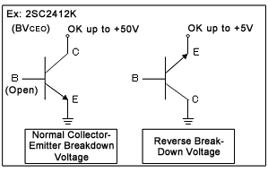
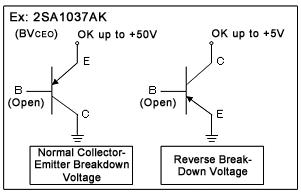
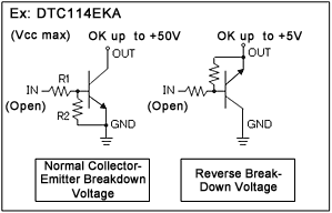
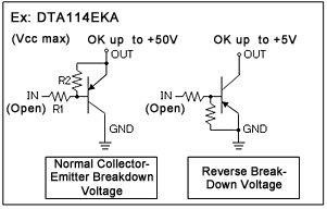
For NPN transistors, VCEO is in breakdown when positive voltage is supplied to the Collector pin while the Emitter is grounded. Conversely, VCEO in PNP transistors is in breakdown when positive voltage is supplied to the Emitter with Collector grounded. Breakdown in the opposite direction (e.g. NPN: +V to Emitter, Collector grounded) is roughly equivalent to the breakdown between the Emitter and Base. Typically this is between 5 to 7V, making the Collector-Emitter reverse voltage less than 5V. (If sufficient voltage is supplied to the Collector-Emitter in reverse, deterioration such as low hFE will occur. Otherwise leakage current will flow.)
The same applies to digital transistors. Voltages up to 5V can be supplied to the Collector-Emitter in the reverse direction as below. However, current flows through what has resistance between an GND terminal and a IN terminal.
The hFE range is depicted in the data sheet. The upper and lower limits for some products are specified while for others only the lower limit is given. The hFE distribution for components with both limits defined will be within the given range, while for transistors with only a lower limit provided the hFE dispersion will be several times the stated lower limit. More detailed information can be obtained by contacting a ROHM sales representative.
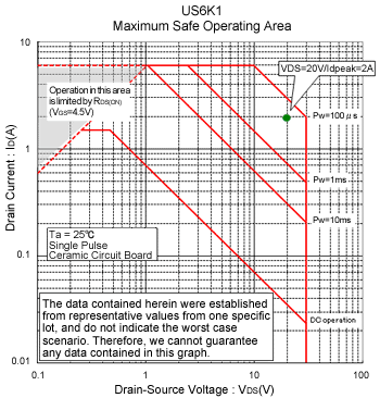
In order to determine the suitability of a transistor is to look at its particular SOA (Safe Operating Area). Ex: In the SOA graph below when VDS is 20Vand IDpeak 2A, making it suitable as long as Pw=100µs or less.
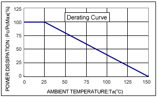
Yes. Pc (Collector power dissipation) must be derated based on the ambient temperature Ta.
Derating must be performed based on the SOA as well. Also, please note that the input voltage (VBE for bipolar and VI(on)/VI(off) for digital) and gain (hFE and G) are affected by the ambient temperature, making it important to verify the electrical characteristics vs. temperature curves (for MOSFETs as well).
In short, no. Transistors and diodes are considered 'articles', or manufactured items formed to a specific shape or design during manufacture which do not release or result in exposure to hazardous chemicals under normal conditions. As such they are exempted from requiring MSDS.
There should be no major differences, similar to small-signal products. However, with power products the thermal resistance may vary depending on rating, even with the same package type.
Although we have been using molded resins containing brominated flame retardants that comply with the RoHS Directive, in order to further reduce environmental impact we will continue to adopt halogen-free resin. ROHM defines halogen-free as (in homogeneous material): 1) Chlorine 900ppm or less 2) Bromine 900ppm or less 3) Total concentrations of chlorine and bromine 1500ppms or less 4) Antimony trioxide 1000ppms or less These specifications comply with the requirements of IEC61249 and are intended to satisfy the stringent environmental management demands of European manufacturers.